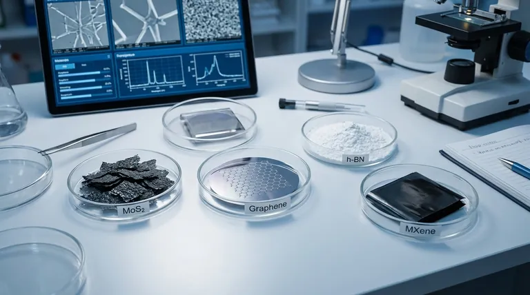
The primary alternatives to graphene are not a single material, but rather a class of two-dimensional (2D) materials, each offering unique properties where graphene falls short. The most prominent alternatives include transition metal dichalcogenides (TMDs) like MoS₂, hexagonal boron nitride (h-BN), phosphorene, and MXenes. Each serves a different purpose, from semiconducting to insulating, that complements or replaces graphene depending on the specific application.
The search for a "graphene alternative" is not about finding a superior material, but about selecting the right tool for the job. Graphene is a benchmark for conductivity and strength, but its lack of a natural bandgap is a critical flaw for digital electronics, driving the exploration of other 2D materials that fill this and other functional gaps.
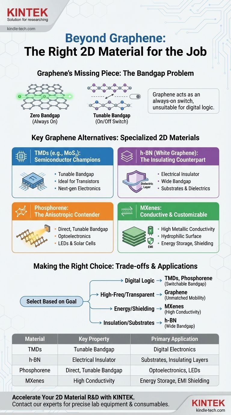
Why Look Beyond Graphene?
Graphene is a revolutionary material, boasting extraordinary electrical conductivity, mechanical strength, and thermal performance. However, its single most significant limitation is its zero-bandgap electronic structure.
The Bandgap Problem
In simple terms, a material's bandgap determines its ability to switch electrical current "on" and "off." Materials with a bandgap are semiconductors, the foundation of all modern digital electronics like transistors and processors.
Because graphene is a semi-metal with no bandgap, it acts like a switch that is always "on." This makes it fundamentally unsuitable for building logic circuits, which is the primary reason the scientific community is actively researching alternatives.
A Tour of Key Graphene Alternatives
Each alternative 2D material offers a unique set of properties, making it a specialist for certain applications where graphene is not the optimal choice.
Transition Metal Dichalcogenides (TMDs): The Semiconductor Champions
TMDs, such as molybdenum disulfide (MoS₂) and tungsten diselenide (WSe₂), represent the most promising class of alternatives for electronics.
Their defining feature is the presence of a natural, tunable bandgap. This allows them to be fabricated into field-effect transistors that can be effectively switched on and off, a feat that is incredibly difficult with pure graphene. This makes TMDs leading candidates for next-generation, ultra-thin electronics and optoelectronics.
Hexagonal Boron Nitride (h-BN): The Insulating Counterpart
Often called "white graphene," h-BN has an atomic structure that is nearly identical to graphene's hexagonal lattice.
However, its electronic properties are the exact opposite. While graphene is an exceptional conductor, h-BN is a superior electrical insulator with a very wide bandgap. This makes it a perfect complementary material, often used as an ultra-flat substrate or a dielectric insulating layer for graphene-based electronic devices.
Phosphorene: The Anisotropic Contender
Phosphorene is a single layer of black phosphorus. Its most unique characteristic is its anisotropy, meaning its electronic and optical properties change depending on the direction of measurement along the material.
This puckered, honeycomb structure results in a direct bandgap, which is highly desirable for optical devices like LEDs and solar cells. Furthermore, this bandgap can be tuned by changing the number of layers, offering another degree of freedom for device engineers.
MXenes: The Conductive and Customizable Family
MXenes (pronounced "max-eens") are a large family of 2D transition metal carbides and nitrides. Unlike graphene, they combine high metallic conductivity with a hydrophilic (water-loving) surface.
This hydrophilic nature makes them much easier to process and mix into solutions or composites. This unique combination of properties makes them exceptionally well-suited for applications in energy storage (supercapacitors, batteries), electromagnetic interference (EMI) shielding, and conductive inks.
Understanding the Critical Trade-offs
Choosing a 2D material requires a clear understanding of its inherent compromises. No single material is perfect for every application.
The Conductor vs. Semiconductor Dilemma
The most fundamental trade-off is the bandgap.
- Graphene: Zero bandgap. Elite for transparent conductors, antennas, and high-frequency electronics but poor for digital logic.
- TMDs & Phosphorene: Natural bandgap. Excellent for transistors and digital logic but have lower charge carrier mobility (slower electron movement) than graphene.
- MXenes: High conductivity (like a metal). Suited for energy and shielding applications, not digital logic.
- h-BN: Wide bandgap. An insulator, used to support and separate other active materials.
Stability and Production Scalability
A significant real-world challenge is material stability. Phosphorene and many MXenes degrade quickly when exposed to air and water, requiring protective encapsulation that adds complexity and cost. Graphene and h-BN are far more stable in ambient conditions.
Furthermore, the cost-effective production of large, defect-free, single-crystal sheets remains a major hurdle for all 2D materials, including graphene. This is the primary barrier to their widespread commercial adoption.
Making the Right Choice for Your Goal
Selecting the correct material depends entirely on your primary objective. The growing family of 2D materials is a toolbox, and you must choose the instrument best suited for your task.
- If your primary focus is digital electronics (transistors): Your best options are TMDs or phosphorene due to their inherent, switchable bandgaps.
- If your primary focus is high-frequency electronics or transparent conductors: Graphene remains the benchmark due to its unmatched electron mobility.
- If your primary focus is energy storage (batteries, supercapacitors) or EMI shielding: MXenes are a leading choice because of their excellent conductivity and ease of processing.
- If your primary focus is creating ultra-flat substrates or insulating layers: Hexagonal boron nitride is the ideal material for the job.
Ultimately, the future of advanced electronics and materials science lies not in a single miracle material, but in learning how to integrate the specialized strengths of each of these remarkable 2D structures.
Summary Table:
| Alternative Material | Key Property | Primary Application |
|---|---|---|
| TMDs (e.g., MoS₂) | Tunable Bandgap | Digital Electronics, Transistors |
| Hexagonal Boron Nitride (h-BN) | Electrical Insulator | Substrates, Insulating Layers |
| Phosphorene | Direct, Tunable Bandgap | Optoelectronics, LEDs |
| MXenes | High Conductivity, Hydrophilic | Energy Storage, EMI Shielding |
Ready to integrate the right 2D material into your research or product development?
At KINTEK, we specialize in providing high-quality lab equipment and consumables tailored for advanced materials science. Whether you're working with graphene, TMDs, MXenes, or other 2D materials, our solutions support precise synthesis, characterization, and application testing.
Let us help you:
- Accelerate your R&D with reliable equipment for material processing and analysis.
- Achieve consistent results with consumables designed for cutting-edge materials.
- Scale your innovations from lab to market with trusted support.
Contact our experts today to discuss your specific needs and discover how KINTEK can empower your next breakthrough in 2D materials.
Visual Guide
Related Products
- Round Bidirectional Press Mold for Lab
- Laboratory CVD Boron Doped Diamond Materials
- Square Lab Press Mold for Laboratory Applications
- Conductive Carbon Cloth Carbon Paper Carbon Felt for Electrodes and Batteries
- Cylindrical Press Mold with Scale for Lab
People Also Ask
- How to use a press mould? Master the Art of Consistent Ceramic Forms
- How to use a press mold? Master the Art of Creating Consistent Ceramic Forms
- What is the purpose of specialized pressure devices in sulfide solid-state batteries? Ensure Chemo-Mechanical Stability
- What is a press mold used for? Achieve Repeatable Precision and Efficiency
- What are the advantages of using bi-directional pressing graphite molds? Achieve Superior Density and Precision