Physical Vapor Deposition (PVD)
PVD Deposition Process
The Physical Vapor Deposition (PVD) process is a sophisticated technique used to deposit thin films on various substrates. This process can be conceptually divided into three primary stages: vaporization, migration, and deposition.
-
Vaporization: The initial stage involves converting the plating material into a gaseous state. This is typically achieved through thermal evaporation or sputtering. In thermal evaporation, the material is heated to its vaporization point, transforming it into a gas. In contrast, sputtering involves bombarding a target material with high-energy particles, such as argon ions, to dislodge and vaporize the material.
-
Migration: Once vaporized, the material particles migrate through the vacuum or low-pressure environment. This migration can be influenced by various factors, including the pressure, temperature, and presence of any reactive gases. The particles travel in a controlled manner towards the substrate where they will eventually deposit.
-
Deposition: Upon reaching the substrate, the vaporized material condenses and forms a thin film. This stage is crucial for the quality and properties of the final coating. The deposition process can be further enhanced by reactive deposition, where the vaporized material reacts with gases in the environment to form compound materials like titanium nitride (TiN) or silicon dioxide (SiO2).
The PVD process is versatile, capable of depositing materials ranging from simple elements to complex alloys and compounds. It is widely used in various industries for applications that require precise control over film thickness, composition, and uniformity.
Types of PVD Methods
Physical Vapor Deposition (PVD) encompasses a variety of techniques, each with its unique mechanisms and applications. The primary methods include:
-
Vacuum Vapor Deposition: This technique involves evaporating materials under vacuum conditions, allowing them to deposit on the substrate surface. It is particularly useful for creating thin, uniform films.
-
Sputtering Coating: In this method, argon gas is ionized to create argon ions that bombard the cathode target. This bombardment causes material to sputter off and deposit onto the workpiece, offering a controlled and efficient coating process.
-
Arc Plasma Coating: This technique utilizes arc discharge between the anode and cathode to generate arc plasma. The plasma rapidly deposits material onto the substrate, making it ideal for applications requiring high deposition rates.
-
Ion Plating: Ion plating involves ionizing the plating material and depositing it on the substrate under a deep negative bias. This method enhances adhesion and film density, making it suitable for a wide range of applications.
-
Molecular Beam Epitaxy (MBE): MBE is a sophisticated technique that involves directing a beam of atoms or molecules onto a heated substrate. It is known for its precision and is often used in the production of high-quality semiconductor films.
Each of these methods has its own set of advantages and is chosen based on the specific requirements of the application, such as film thickness, uniformity, and adhesion.
Vacuum Vapor Deposition
Vacuum vapor deposition, a subset of Physical Vapor Deposition (PVD), involves the meticulous process of evaporating materials under highly controlled vacuum conditions. This method ensures that the material being deposited is free from any atmospheric interference, enabling precise layering on the substrate surface. The vacuum environment is crucial as it minimizes the presence of gas molecules, facilitating the deposition of material on an atomic or molecular level.
The layers formed through this process can range from a single atom to several millimeters in thickness, providing a versatile range for various applications. The process can be further categorized based on the vapor source: physical vapor deposition uses a liquid or solid source, while chemical vapor deposition employs a chemical vapor.
In vacuum vapor deposition, the material is typically heated until it vaporizes, and the resulting vapor condenses on the substrate, forming a thin film. This technique is widely used in the deposition of both metals (such as cadmium, chromium, copper, nickel, and titanium) and nonmetals (like ceramic matrix composites of carbon/carbon and carbon/silicon carbide). The deposition occurs atom by atom or molecule by molecule, ensuring a high degree of control and uniformity in the resulting film.
The advantages of conducting this process in a vacuum include:
- Minimized Contamination: The absence of atmospheric gases reduces the risk of impurities in the deposited film.
- Enhanced Control: Precise control over the deposition process allows for the creation of highly uniform and consistent films.
- Reduced Processing Temperature: The vacuum environment can lower the required processing temperature, which is beneficial for heat-sensitive substrates.
This method is integral in various industries, including electronics, optics, and aerospace, where the quality and precision of thin films are paramount.
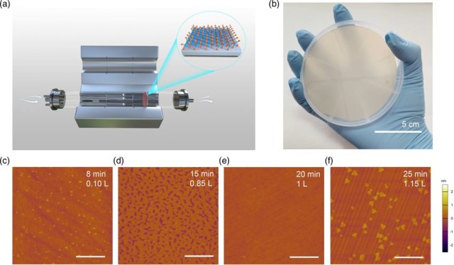
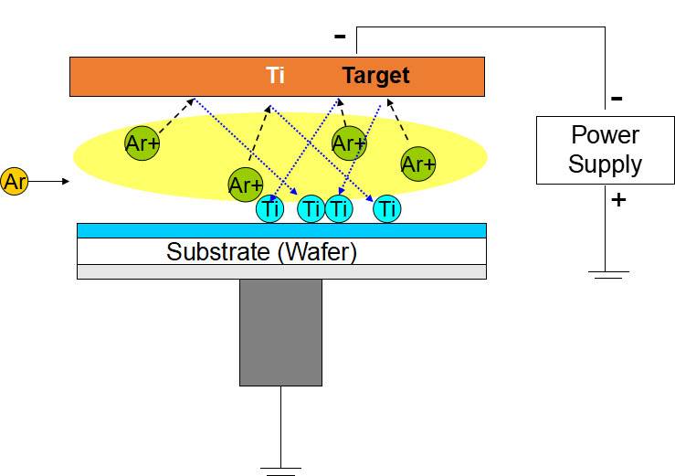
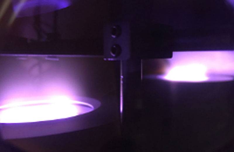
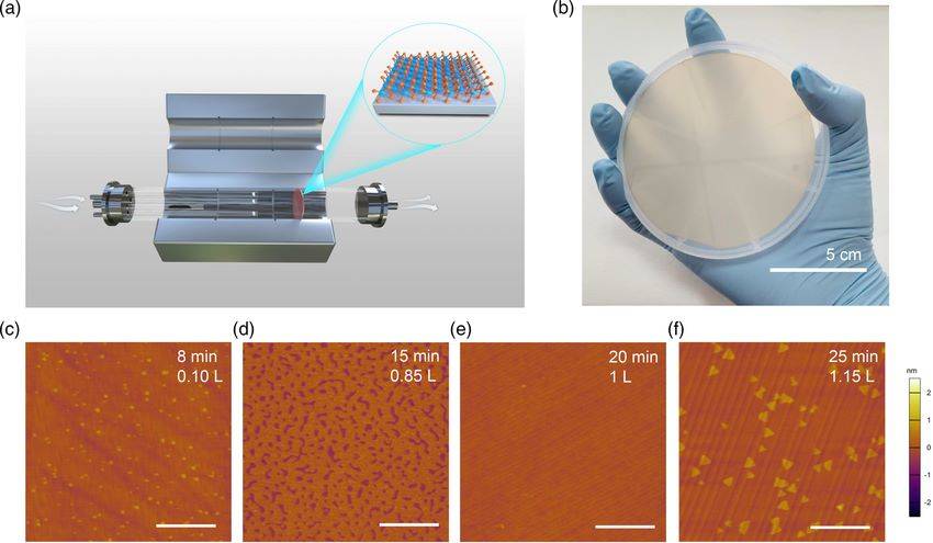
Sputtering Coating
Sputtering coating is a sophisticated physical vapor deposition (PVD) process designed to apply a thin, functional layer onto a substrate. This technique begins with the ionization of argon gas, creating high-energy argon ions that are directed towards a cathode target. The bombardment of these ions causes the target material to be ejected from its surface, a phenomenon known as sputtering. The sputtered material then migrates and deposits onto the workpiece, forming a durable and tightly bonded coating.
The process is meticulously controlled, often utilizing magnets to ensure uniform erosion of the target material. This uniformity is crucial for achieving consistent film thickness and quality across the substrate. At a molecular level, the sputtered material undergoes a momentum transfer process, where it is propelled towards the substrate with sufficient energy to penetrate its surface. This energetic interaction results in a strong atomic-level bond, effectively integrating the coating into the substrate rather than merely adhering to its surface.
In specialized applications, such as in Scanning Electron Microscopy (SEM), sputter coating is enhanced to provide an electrically conductive thin film that accurately represents the specimen. This enhancement addresses common challenges in SEM, such as charging, thermal damage, and the emission of secondary electrons, thereby improving the quality and reliability of the imaging process.
Arc Plasma Coating
Arc plasma coating is a sophisticated Physical Vapor Deposition (PVD) technique that relies on the arc discharge phenomenon between an anode and a cathode. This method is particularly notable for its ability to rapidly deposit materials onto substrates, making it a preferred choice in various industrial applications.
The process begins with the creation of an electrical arc, which ionizes the surrounding gas and generates a high-energy plasma. This plasma, composed of highly energetic particles, is then directed towards the substrate. The intense heat and energy from the arc cause the material at the cathode to evaporate, forming a vapor that is subsequently condensed onto the substrate. This rapid deposition ensures a uniform and dense coating, which is crucial for enhancing the durability and performance of the coated components.
Arc plasma coating is versatile, capable of depositing a wide range of materials, including titanium nitride, zirconium nitride, and silver, among others. The flexibility in material selection allows for tailored coatings that meet specific functional requirements, whether it be improving wear resistance, enhancing electrical conductivity, or providing aesthetic finishes.
In comparison to other PVD methods, arc plasma coating stands out due to its high deposition rates and the ability to handle complex geometries. Unlike Atomic Layer Deposition (ALD), which is excellent for precise control over coating thickness but limited by its slower deposition rates, arc plasma coating offers a balance between speed and precision. This makes it particularly suitable for applications where rapid production is essential without compromising on the quality of the coating.
Moreover, arc plasma coating, especially when practiced as low-temperature arc vapor deposition (LTAVD), can achieve a variety of aesthetic finishes, ranging from hues of black, bronze, gold, to more intricate "rainbow" combinations. This aesthetic versatility, combined with its functional benefits, underscores the broad applicability of arc plasma coating across industries such as automotive, aerospace, and consumer electronics.
Ion Plating
Ion plating is a sophisticated deposition technique that involves the ionization of the plating material, which is then deposited onto the substrate under a deep negative bias. This method leverages energetic particle bombardment, typically ions of an inert or reactive gas or ions of the depositing material, to modify and control the properties of the deposited film. This bombardment enhances surface coverage and adhesion, making ion plating particularly effective for applications requiring robust coatings.
The process can be executed in two primary environments: plasma-based and vacuum-based. In plasma-based ion plating, ions for bombardment are extracted from the plasma, while in vacuum-based ion plating, ions are formed in a separate ion gun. The latter configuration is often referred to as ion beam assisted deposition (IBAD).
Key Advantages and Disadvantages
| Advantages | Disadvantages |
|---|---|
| - Enhanced Adhesion: The energetic particle bombardment significantly improves the adhesion of the deposited film to the substrate. | - Controlled Processing: Requires tightly controlled processing parameters to ensure consistent results. |
| - Surface Finish: Provides a superior surface finish compared to other deposition methods. | - Potential Contamination: Risk of contamination from activated plasma or bombarded gas species. |
| - In-situ Cleaning: Allows for the cleaning of the substrate prior to film deposition, ensuring a clean surface for better coating quality. | - Complexity: More complex and expensive compared to simpler deposition techniques. |
| - Tailorable Properties: The properties of the deposited film, such as morphology, density, and residual stress, can be tailored to specific requirements. |
Applications
Ion plating finds extensive use in various industries due to its ability to produce high-quality coatings. Some typical applications include:
- X-ray Tubes: Providing durable coatings that enhance the performance and longevity of X-ray tubes.
- Aircraft Engine Turbine Blades: Protecting turbine blades from high-temperature corrosion and wear.
- Steel Drill Bits: Enhancing the durability and performance of drill bits used in demanding drilling operations.
- Decorative Coatings: Applying aesthetic and protective coatings to various consumer products.
- Corrosion Protection: Offering robust corrosion protection in critical environments such as nuclear reactors.
In summary, ion plating is a versatile and powerful deposition technique that offers significant advantages in terms of coating quality and adhesion, making it indispensable in several high-tech industries.
Chemical Vapor Deposition (CVD)
CVD Process Overview
Chemical Vapor Deposition (CVD) is a sophisticated technique that involves high-temperature gas-phase reactions to precipitate a wide array of inorganic materials, including metals, oxides, and carbides. This process is pivotal in the deposition of thin films, which are integral to various industries such as electronics, optoelectronics, and thin film coatings.
The CVD process can be categorized into several specialized methods, each tailored to specific applications and material properties:
- Atmospheric Pressure Chemical Vapour Deposition (APCVD): Operates at atmospheric pressure, making it suitable for large-scale production.
- Low Pressure Chemical Vapour Deposition (LPCVD): Conducted under reduced pressure, enhancing uniformity and thickness control.
- Metal-Organic Chemical Vapour Deposition (MOCVD): Utilizes metal-organic precursors, ideal for depositing complex compound films.
- Plasma Assisted Chemical Vapour Deposition (PACVD) or Plasma Enhanced Chemical Vapour Deposition (PECVD): Incorporates plasma to facilitate reactions at lower temperatures, particularly useful for amorphous silicon (a-Si) films and protective coatings.
- Laser Chemical Vapour Deposition (LCVD): Employs laser energy to induce localized deposition, offering precise control over film properties.
- Photochemical Vapour Deposition (PCVD): Uses photochemical reactions to deposit films, often in conjunction with other techniques.
- Chemical Vapour Infiltration (CVI): Focuses on infiltrating porous substrates with reactive gases to form dense coatings.
- Chemical Beam Epitaxy (CBE): Utilizes molecular beams to achieve highly controlled epitaxial growth.
Each of these methods has unique advantages and is chosen based on the desired film properties, deposition rate, and specific application requirements. The versatility of CVD allows for the creation of thin films with tailored properties, making it an indispensable tool in modern technology.
Basic Chemical Reaction Processes
The Chemical Vapor Deposition (CVD) process encompasses a variety of chemical reactions that facilitate the deposition of inorganic thin films. These reactions can be broadly categorized into several key processes:
-
Pyrolysis: This involves the thermal decomposition of precursor molecules at elevated temperatures, leading to the formation of solid film on the substrate. Pyrolysis is crucial for the deposition of materials like silicon dioxide (SiO₂) and silicon nitride (Si₃N₄).
-
Photolysis: In this process, the precursor molecules are decomposed by ultraviolet (UV) light, enabling the deposition of thin films at lower temperatures compared to pyrolysis. Photolysis is often used in applications requiring precise control over film thickness and uniformity.
-
Reduction Reactions: These reactions involve the reduction of metal compounds to form metal films. For instance, the reduction of tungsten hexafluoride (WF₆) with hydrogen (H₂) results in the deposition of tungsten (W).
-
Oxidation Reactions: Here, the precursor molecules react with oxygen to form oxide films. An example is the oxidation of silicon tetrachloride (SiCl₄) to produce silicon dioxide (SiO₂).
-
Redox Reactions: These are simultaneous reduction and oxidation processes, often involving the interaction of a metal precursor with a reducing agent and an oxidizing agent. Redox reactions are essential for the deposition of complex thin films with multiple components.
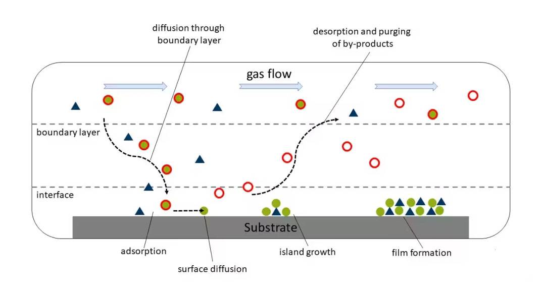
Each of these reaction processes plays a vital role in the CVD technique, enabling the precise control and deposition of a wide range of inorganic materials.
Types of CVD Reactive Sources
Chemical Vapor Deposition (CVD) employs a variety of reactive sources to facilitate the deposition of inorganic thin films. These sources can be categorized into three primary states: gaseous, liquid, and solid. Each state presents unique characteristics and necessitates distinct control mechanisms to ensure effective and precise film deposition.
Gaseous Reactive Sources
Gaseous sources are typically used in high-temperature CVD processes. They offer the advantage of being easily transported and mixed within the reactor, allowing for uniform distribution of reactants. Common gaseous sources include silane (SiH₄) for silicon deposition and ammonia (NH₃) for nitride films. The control mechanisms for gaseous sources often involve precise flow control and temperature regulation to maintain the desired reaction conditions.
Liquid Reactive Sources
Liquid sources are often used in low-pressure CVD (LPCVD) and metal-organic CVD (MOCVD) processes. They provide a convenient means of delivering complex precursors that can be volatilized into a gas phase. For instance, metal-organic precursors like trimethylgallium (TMG) are used in the production of III-V semiconductor materials. The control of liquid sources requires sophisticated vaporization systems and pressure control to ensure the precursor is delivered at the correct concentration and flow rate.
Solid Reactive Sources
Solid sources are typically used in processes like atomic layer deposition (ALD) and some specialized CVD techniques. They often involve the sublimation of solid precursors into a gas phase. Examples include aluminum trichloride (AlCl₃) for aluminum oxide deposition. The control mechanisms for solid sources are more complex, involving precise temperature control and sublimation rates to maintain the precursor's stability and reactivity.
Each type of reactive source brings its own set of challenges and advantages, necessitating tailored control strategies to optimize the deposition process. By understanding these differences, researchers and engineers can better select and implement the appropriate CVD reactive sources for specific applications.
Plasma Enhanced Chemical Vapor Deposition (PECVD)
Plasma Enhanced Chemical Vapor Deposition (PECVD) represents a significant advancement in the field of thin film deposition, particularly in the realm of semiconductor manufacturing and display technology. Unlike conventional Chemical Vapor Deposition (CVD) methods, which rely solely on substrate temperature to drive chemical reactions, PECVD harnesses the power of plasma to facilitate these reactions at significantly lower temperatures. This innovative approach not only reduces thermal stress on the substrate but also enhances deposition rates, making it an ideal choice for applications requiring precise control and uniformity.
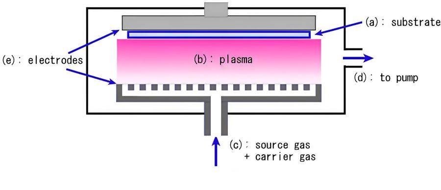
The process begins with the introduction of reactive gas species into a reactor chamber, where they are subjected to an electric field that ionizes the gas, creating a plasma. Energetic electrons within this plasma environment provide the necessary activation energy for the chemical reactions to occur, thereby circumventing the limitations imposed by thermal energy alone. This plasma-driven mechanism allows for the deposition of high-quality thin films at temperatures ranging from 200 to 400°C, as opposed to the higher temperatures required by traditional CVD methods, which typically range between 425 and 900°C.
PECVD is particularly well-suited for the deposition of silicon-based films, such as amorphous silicon (a-Si), silicon nitride (SiNx), and silicon dioxide (SiO2), which are critical components in various electronic devices. For instance, in display manufacturing, PECVD is employed to create gate insulating films, protective films, and active layers in thin-film transistors (TFTs), ensuring superior performance and reliability. The ability to deposit these films with excellent uniformity across different substrates, including optical glass, silicon, quartz, and stainless steel, further underscores the versatility and efficacy of PECVD in modern fabrication processes.
In summary, PECVD leverages the unique properties of plasma to achieve efficient and high-quality thin film deposition at reduced temperatures, making it an indispensable technique in the production of advanced electronic devices and displays.
Atomic Layer Deposition (ALD)
Atomic Layer Deposition (ALD) is a specialized form of Chemical Vapor Deposition (CVD) that excels in producing ultra-thin, highly uniform, and conformal films. This technique relies on sequential, self-limiting chemical reactions between gas-phase precursors and the substrate surface, ensuring precise control over film thickness at the atomic level.
One of the hallmarks of ALD is its ability to achieve exceptional step coverage, even over features with aspect ratios approaching 2000:1. This capability makes ALD particularly valuable in applications requiring intricate and complex film geometries, such as in the semiconductor industry. For instance, the use of trimethylaluminum (TMA) and water vapor (H2O) can yield aluminum oxide (Al2O3) films with remarkable uniformity and density.
ALD operates through a series of pulse and purge steps, where precursors are introduced sequentially into the reaction chamber, ensuring that no two precursors are present simultaneously. This methodical process allows for the growth of films with thicknesses ranging from 0.04nm to 0.10nm per cycle, making it possible to deposit layers thinner than 10nm with predictable precision. The repeatability of the ALD process is another key advantage, enabling the creation of consistent and reliable thin films.
In addition to aluminum oxide, ALD can also deposit other materials such as hafnium oxide (HfO2) and titanium oxide (TiO2), broadening its applicability across various industries including microelectromechanical systems (MEMS), catalysis, and nanotechnology. Despite its slow deposition rate, the unparalleled control and uniformity offered by ALD make it an indispensable tool in advanced material science and engineering.
Applications and Comparisons
PVD Applications in Display Production
Physical Vapor Deposition (PVD) technology plays a crucial role in the production of advanced display technologies, particularly in the fabrication of Active Matrix Organic Light Emitting Diodes (AMOLEDs) and other high-performance displays. In AMOLEDs, PVD is employed for the deposition of active metal electrodes, which are essential for the efficient operation of the display. These electrodes facilitate the injection of charge carriers into the organic layers, enabling the emission of light.
Additionally, PVD is utilized for the deposition of small molecules that form the organic layers within AMOLEDs. These molecules are carefully deposited to ensure uniform light emission and high contrast ratios. Furthermore, PVD is instrumental in the creation of pixel electrodes, where it is used to deposit metals and Indium Tin Oxide (ITO), a transparent conductive material that is critical for the functionality of the display.
The application of PVD in display production extends beyond AMOLEDs. It is also used in the fabrication of other display technologies, such as Liquid Crystal Displays (LCDs) and Quantum Dot Displays (QDs), where it ensures the deposition of high-quality, thin films that enhance the overall performance and durability of the displays. These thin films are essential for fulfilling various mechanical, optical, and electronic functions, such as improving reflectivity, enhancing durability, and ensuring efficient charge transport.
Despite its numerous advantages, PVD has some limitations. For instance, the technology often struggles with coating the back and sides of tools due to low air pressure within the PVD reactor. To mitigate this issue, the reactor must be loaded at a reduced density to avoid shadowing effects, which complicates the loading and fixing processes. Additionally, the costs associated with PVD can be high, particularly when dealing with complex display structures.
Overall, PVD remains a vital technology in the display industry, contributing to the advancement of high-performance displays through precise and efficient thin film deposition processes.
CVD Applications in Display Production
Chemical Vapor Deposition (CVD), with its advanced variant Plasma Enhanced Chemical Vapor Deposition (PECVD), plays a pivotal role in the production of display technologies. PECVD is particularly favored for its ability to deposit silicon-bearing layers such as amorphous silicon (a-Si), silicon dioxide (SiO2), and silicon nitride (SiNx) at relatively lower temperatures compared to traditional CVD methods.
In the context of display manufacturing, these silicon-based layers are crucial for several key components:
- Amorphous Silicon (a-Si): Used extensively in thin-film transistors (TFTs) for active matrix displays, a-Si provides the necessary electrical conductivity and stability.
- Silicon Dioxide (SiO2): Often employed as a dielectric layer, SiO2 offers excellent insulation properties, protecting underlying layers from electrical shorts.
- Silicon Nitride (SiNx): This material is frequently utilized as a barrier layer, enhancing the durability and performance of the display by preventing moisture and gas penetration.
The versatility of PECVD in creating these layers is further complemented by its efficiency in semiconductor manufacturing. For instance, in the production of solar cells, PECVD is used to grow silicon layers on monocrystalline silicon substrates, forming layers that are typically 15-50 microns thick. This application not only underscores the scalability of PECVD but also its adaptability across different industries.
In summary, PECVD's ability to produce high-quality, silicon-bearing layers at lower temperatures makes it an indispensable tool in modern display production, ensuring the performance, durability, and efficiency of various display components.
Advantages and Disadvantages of ALD
Atomic Layer Deposition (ALD) is celebrated for its unparalleled film uniformity and high film density, which are critical for achieving precise and consistent thin film properties. However, the method is not without its limitations, particularly in industrial production where the low deposition rate can be a significant bottleneck.
Advantages
- Uniformity: ALD excels in creating films with exceptional uniformity across large substrates, a feature that is particularly important in applications like semiconductor manufacturing and display production.
- High Film Density: The self-limiting nature of ALD reactions ensures high film density, leading to robust and durable coatings that are resistant to defects and pinholes.
Disadvantages
- Low Deposition Rate: One of the most notable drawbacks of ALD is its relatively slow deposition rate. This limitation can significantly extend production times, making it less efficient for large-scale industrial applications compared to other CVD methods.
- Process Complexity: The precise control required for ALD processes adds complexity to the equipment and operational procedures, which can increase costs and require highly skilled operators.
These advantages and disadvantages highlight the trade-offs involved in choosing ALD for specific applications, emphasizing the need for careful consideration based on the requirements of the manufacturing process.
Related Products
- Chemical Vapor Deposition CVD Equipment System Chamber Slide PECVD Tube Furnace with Liquid Gasifier PECVD Machine
- Customer Made Versatile CVD Tube Furnace Chemical Vapor Deposition Chamber System Equipment
- HFCVD Machine System Equipment for Drawing Die Nano-Diamond Coating
- Split Chamber CVD Tube Furnace with Vacuum Station Chemical Vapor Deposition System Equipment Machine
- Multi Heating Zones CVD Tube Furnace Machine Chemical Vapor Deposition Chamber System Equipment


