Preparation Processes for Silicon Nitride Films
Low Pressure Chemical Vapor Deposition (LPCVD)
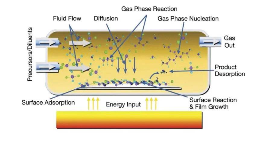
Low Pressure Chemical Vapor Deposition (LPCVD) is a sophisticated deposition technique that operates under reduced pressure, typically around 133 Pa or lower. This method leverages a high thermal environment to enhance gas diffusion and the mean free path within the reaction chamber, leading to superior film uniformity and resistivity uniformity. The low pressure setting accelerates the gas transport rate, allowing impurities and by-products to be swiftly removed from the reaction zone, thereby minimizing self-doping and boosting production efficiency.
Advantages:
- Film Thickness Uniformity: LPCVD excels in producing films with excellent thickness uniformity across large substrates, making it ideal for applications requiring consistent film properties.
- High Repeatability: The process offers high repeatability, ensuring that each deposition run yields similar results, which is crucial for mass production in the semiconductor industry.
- Enhanced Trench Coverage: The improved gas diffusion and mean free path contribute to better trench coverage and filling capabilities, crucial for intricate device structures.
Disadvantages:
- Higher Deposition Temperature: LPCVD requires higher deposition temperatures, which can impose thermal stress on the substrate and necessitate more robust equipment.
- Equipment Requirements: The need for precise temperature and pressure control necessitates advanced and expensive equipment, adding to the overall cost of the process.
- Narrower Process Window: The process window for LPCVD is relatively narrow, making it more sensitive to variations in process parameters, which can complicate process optimization and control.
LPCVD is widely employed in the semiconductor industry for the deposition of high-value thin films, particularly for applications such as resistors, capacitor dielectrics, MEMS, and anti-reflective coatings. Despite its challenges, LPCVD remains a preferred method for its ability to deliver high-quality, uniform films with minimal defects.
Plasma Enhanced Chemical Vapor Deposition (PECVD)
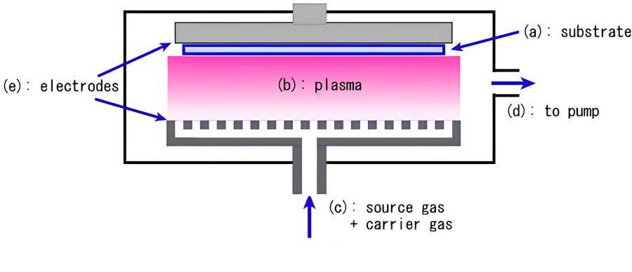
Plasma Enhanced Chemical Vapor Deposition (PECVD) stands out as a versatile method for depositing thin films at significantly reduced temperatures compared to traditional Low Pressure Chemical Vapor Deposition (LPCVD). This technique leverages the energy from a plasma to activate the deposition process, allowing for the creation of films such as silicon nitride, amorphous silicon, and microcrystalline silicon on a variety of substrates including optical glass, silicon, quartz, and stainless steel.
Advantages
One of the key benefits of PECVD is its ability to operate at lower temperatures, typically ranging between 200-400°C, as opposed to the 425-900°C range required for LPCVD. This lower temperature regime minimizes thermal damage to the substrate, making it particularly suitable for delicate materials. Additionally, PECVD enables the deposition of large-area amorphous films, which is crucial for applications requiring uniform coatings over extensive surfaces.
Disadvantages
Despite its advantages, PECVD is not without its challenges. The film thickness uniformity achieved through PECVD is generally inferior to that of LPCVD, primarily due to the sensitivity of the process to plasma parameters. This sensitivity can lead to the generation of defects, which can compromise the integrity and performance of the deposited films. Moreover, the variability in plasma conditions necessitates meticulous control and monitoring to ensure consistent results.
In summary, while PECVD offers a compelling solution for low-temperature film deposition with minimal substrate damage, its application is tempered by the need for precise plasma management and the potential for reduced film uniformity.
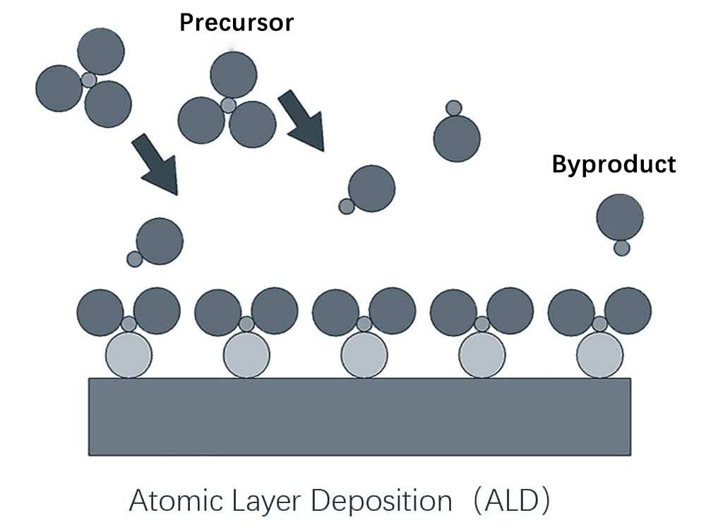
Atomic Layer Deposition (ALD)
Atomic Layer Deposition (ALD) stands out as a unique Chemical Vapor Deposition (CVD) technique, renowned for its ability to achieve surface-controlled, uniform, and highly conformal film growth at the atomic layer scale. This precision is rooted in the sequential, self-limiting chemical reactions between gas-phase precursor molecules and active surface species. A typical ALD process involves the sequential pulsing of at least two gas-phase precursors into a reaction space containing a substrate. For instance, the combination of trimethylaluminum (TMA) and water vapor (H2O) can yield high-quality aluminum oxide (Al2O3) films. Each ALD cycle consists of a series of pulse and purge steps, meticulously designed to remove any residual precursor or volatile by-products, ensuring a clean reaction environment.
The meticulous control inherent in ALD processes allows for the deposition of films with exceptional uniformity and conformality, even over features with aspect ratios approaching 2000:1. This capability ensures excellent step coverage, making ALD particularly advantageous for applications requiring ultra-thin layers, often below 10nm in thickness. The repeatability of the ALD process enables predictable growth of these thin layers, a feature that has significantly advanced its adoption in the semiconductor industry for developing high-K gate dielectric layers.
Despite its many advantages, ALD is not without its challenges. The primary drawbacks include a relatively slow deposition rate, which can be as low as 0.04nm to 0.10nm of film thickness per cycle, and a higher operational cost due to the stringent requirements for precursor purity and the need for precise temperature control, typically around 180°C. These factors, while limiting the throughput and increasing the cost, are nevertheless justified by the unparalleled precision and quality of the films produced.
In summary, while ALD's slow deposition rate and higher cost present practical challenges, its unparalleled precision in film thickness control, atomic-level thickness management, and superior film uniformity make it an indispensable tool in advanced semiconductor manufacturing and nanotechnology applications.
Factors Affecting Thickness Control Accuracy
Process Parameters
The accuracy of film thickness control in silicon nitride film preparation processes is profoundly influenced by several key process parameters. These parameters, including deposition time, gas flow rate, deposition temperature, and pressure, each play a critical role in determining the final uniformity and precision of the film.
Deposition Time: The duration of the deposition process directly affects the total thickness of the film. Longer deposition times generally result in thicker films, but maintaining precise control over time is essential to avoid inconsistencies.
Gas Flow Rate: The rate at which precursor gases are introduced into the deposition chamber impacts the reaction rate and, consequently, the film's growth rate. A stable and controlled gas flow rate is crucial for achieving uniform film thickness across the substrate.
Deposition Temperature: The temperature at which the deposition occurs significantly influences the chemical reactions involved in film formation. Higher temperatures often lead to faster deposition rates but can also introduce thermal stress and affect the film's structural integrity.
Pressure: The pressure within the deposition chamber governs the mean free path of gas molecules and the overall reaction environment. Optimal pressure settings are necessary to ensure that the film grows uniformly without defects or pinholes.
These parameters are interdependent, and their optimal settings vary depending on the specific deposition technique employed, whether it be Low Pressure Chemical Vapor Deposition (LPCVD), Plasma Enhanced Chemical Vapor Deposition (PECVD), or Atomic Layer Deposition (ALD). Each technique has its unique process window, and fine-tuning these parameters within that window is essential for achieving the desired film thickness control accuracy.
Equipment Performance
Gas flow control accuracy, temperature control accuracy, and pressure control accuracy are paramount for achieving uniform film thickness in silicon nitride film preparation. These parameters directly influence the consistency and quality of the deposited film, which is critical in semiconductor manufacturing.
| Control Parameter | Importance | Challenges |
|---|---|---|
| Gas Flow Control | Ensures the precise delivery of reactant gases, which is essential for uniform chemical reactions and consistent film growth. | Requires high precision valves and flow meters to maintain exact flow rates. |
| Temperature Control | Maintains the optimal deposition temperature, crucial for the chemical reactions that form the film. High accuracy prevents temperature fluctuations that could lead to non-uniform film thickness. | Needs sophisticated heating and cooling systems with feedback control. |
| Pressure Control | Manages the reaction environment, influencing the rate and uniformity of film deposition. Accurate pressure control ensures consistent process conditions. | Involves complex vacuum systems and pressure regulators. |
Each of these control parameters must be meticulously calibrated and monitored to ensure the highest possible accuracy. Any deviation can result in variations in film thickness, which can compromise the performance and reliability of the semiconductor device. Therefore, the equipment used in these processes must be of the highest quality and precision to meet the stringent requirements of film thickness control.
Film Material Characteristics
The growth rate and internal stress of a film material are critical factors that influence the difficulty and uniformity of film thickness control. These characteristics are not isolated; they are deeply intertwined with the application requirements, which can span categories such as photonic, optical, electronic, mechanical, or chemical. In many cases, films must meet stringent criteria across multiple categories simultaneously.
For instance, the process temperature, which significantly affects film characteristics, can be a limiting factor imposed by the application. High temperatures may enhance the growth rate but could also introduce stress, potentially leading to non-uniform thickness and structural defects. Conversely, lower temperatures might reduce stress but could also slow the growth rate, complicating efforts to achieve the desired film thickness within a practical timeframe.
| Parameter | Impact on Thickness Control |
|---|---|
| Growth Rate | Higher growth rates can lead to faster deposition but may compromise uniformity and structural integrity. |
| Internal Stress | High stress can cause warping or cracking, affecting thickness uniformity and overall film quality. |
| Process Temperature | Temperature control is crucial; higher temperatures can enhance growth but may introduce stress, while lower temperatures can reduce stress but slow growth. |
Balancing these factors requires a nuanced understanding of both the material properties and the specific demands of the application. This balance is essential for achieving the precise and uniform film thickness necessary for optimal performance in semiconductor manufacturing.
Comparison of Thickness Control Accuracy Among Processes
Atomic Layer Deposition (ALD)
Atomic Layer Deposition (ALD) stands out as a premier technique for achieving unparalleled film thickness control accuracy. This precision is rooted in its self-limiting growth method, which allows for the deposition of films with atomic-level thickness control. The process operates through sequential, self-limiting chemical reactions between gas-phase precursor molecules and active surface species, ensuring that each layer is precisely controlled.
One illustrative example of an ALD process involves the use of trimethylaluminum (TMA) and water vapor (H₂O) to grow aluminum oxide (Al₂O₃). Each cycle in the ALD process consists of a series of pulse and purge steps, meticulously designed to remove any residual precursor or volatile by-products from the reaction space. This meticulous approach results in film growth rates as low as 0.04nm to 0.10nm per cycle, necessitating a controlled environment with temperatures around 180°C.
The films produced via ALD are renowned for their exceptional conformality, approaching aspect ratios of 2000:1, which translates to excellent step coverage over intricate features. This high conformality is a critical advantage in applications requiring uniform film deposition, such as in the semiconductor industry where ALD has rapidly advanced to develop thin, high-K gate dielectric layers.
In summary, ALD's unique ability to deposit ultra-thin, highly conformal films in a precisely controlled manner makes it indispensable for applications demanding the highest standards of film thickness control.
Low Pressure Chemical Vapor Deposition (LPCVD)
LPCVD offers exceptional control over film thickness and uniformity by operating at reduced pressures, typically around 133 Pa or less. This low-pressure environment significantly enhances the gas diffusion coefficient and the mean free path within the reaction chamber, leading to superior film uniformity, resistivity uniformity, and trench coverage filling capability. The faster gas transport rate in this environment allows impurities and reaction by-products to be swiftly removed from the reaction zone, while the reaction gas efficiently reaches the substrate surface for deposition. This dynamic process not only suppresses self-doping but also boosts production efficiency.
Moreover, LPCVD's design eliminates the need for carrier gases, thereby minimizing particle contamination sources. This makes LPCVD a preferred method in the high-value semiconductor industry for depositing thin films. The process operates within a pressure range of 0.1 – 10 Torr and temperatures ranging from 200 – 800°C, utilizing a specialized precursor delivery system to ensure precise control over the deposition process. Post-reaction, the by-products are efficiently evacuated using vacuum pumps, ensuring a clean deposition environment.
LPCVD's versatility is further highlighted by its application in the production of resistors, capacitor dielectrics, MEMS, and anti-reflective coatings, demonstrating its broad utility in various semiconductor manufacturing processes.
Plasma Enhanced Chemical Vapor Deposition (PECVD)
Plasma Enhanced Chemical Vapor Deposition (PECVD) stands out as a versatile technique for thin film deposition, particularly suited for materials like silicon nitride, amorphous silicon, and microcrystalline silicon. Unlike conventional Chemical Vapor Deposition (CVD) methods that rely solely on substrate temperature for surface reactions, PECVD leverages plasma to enhance the deposition process. This plasma-assisted approach not only accelerates the deposition rate but also allows for lower processing temperatures, typically ranging between 200-400°C, compared to the higher temperatures required in Low Pressure Chemical Vapor Deposition (LPCVD), which can reach up to 900°C.
However, while PECVD offers significant advantages such as lower temperature processing and the ability to deposit films on a variety of substrates, including optical glass, silicon, quartz, and stainless steel, it is not without its challenges. One of the primary limitations of PECVD is its relatively lower control over film thickness uniformity. This shortcoming is primarily attributed to the sensitivity of the process to plasma parameters. The energetic electrons in the plasma, which drive the deposition process, can introduce variability that is difficult to manage, leading to inconsistencies in film thickness.
Achieving a uniform film thickness in PECVD is particularly challenging due to the dynamic nature of the plasma. The plasma's high-energy environment can cause fluctuations in the deposition rate, making it difficult to maintain a consistent layer thickness across the substrate. Additionally, the complexity of plasma interactions with the precursor gases further complicates the process, often resulting in the formation of defects or non-uniformities in the deposited film.
In summary, while PECVD provides a cost-effective and efficient method for depositing thin films at lower temperatures, its reliance on plasma dynamics introduces significant challenges in achieving precise and uniform film thickness control. This sensitivity to plasma parameters necessitates careful process optimization to mitigate these issues and improve the overall quality of the deposited films.
Choosing the Right Preparation Process
Accuracy Requirements
When it comes to achieving very high film thickness control accuracy in semiconductor manufacturing, Atomic Layer Deposition (ALD) stands out as the preferred method. ALD's unique self-limiting growth mechanism enables it to achieve precision at the atomic level, making it the gold standard for applications where even the slightest variation in film thickness can significantly impact device performance.
Precision at the Atomic Level
ALD's self-limiting nature ensures that each layer of the film is deposited with exacting precision. This method allows for the control of film thickness down to the atomic scale, which is crucial for applications such as advanced logic and memory devices where nanometer-scale accuracy is essential. The ability to deposit ultra-thin films with consistent thickness across large wafers is a key advantage that sets ALD apart from other deposition techniques.
Comparison with Other Methods
While Low Pressure Chemical Vapor Deposition (LPCVD) and Plasma Enhanced Chemical Vapor Deposition (PECVD) offer their own advantages in terms of deposition rate and cost, they fall short in achieving the same level of thickness control as ALD. LPCVD provides high accuracy and good uniformity but requires higher temperatures and has a narrower process window. PECVD, on the other hand, operates at lower temperatures but is more sensitive to plasma parameters, leading to potential defects and less uniform film thickness.
| Deposition Method | Thickness Control Accuracy | Uniformity | Deposition Rate | Cost |
|---|---|---|---|---|
| ALD | Very High | Excellent | Slow | High |
| LPCVD | High | Good | Moderate | Moderate |
| PECVD | Moderate | Fair | Fast | Moderate |
In summary, for applications demanding the utmost precision in film thickness control, ALD remains the superior choice despite its higher cost and slower deposition rate. Its ability to deliver atomic-level accuracy makes it indispensable in the production of cutting-edge semiconductor devices.
Deposition Rate
When considering the deposition rate for large-area films, both Low Pressure Chemical Vapor Deposition (LPCVD) and Plasma Enhanced Chemical Vapor Deposition (PECVD) emerge as the preferred methods. Each of these techniques offers distinct advantages that make them suitable for rapid film formation across extensive substrates.
LPCVD: Speed and Uniformity
LPCVD excels in its ability to achieve rapid deposition rates while maintaining a high level of film thickness uniformity. This process is particularly advantageous for applications requiring large-area coverage, where consistent film properties are crucial. The trade-off, however, lies in the higher deposition temperatures and the elevated equipment requirements, which can limit the process window and increase operational costs.
PECVD: Temperature Efficiency and Versatility
On the other hand, PECVD offers a significant advantage in terms of lower deposition temperatures, making it an ideal choice for substrates that are sensitive to thermal damage. This method enables the deposition of amorphous films at low temperatures, which is particularly beneficial for maintaining substrate integrity. Despite its lower film thickness uniformity compared to LPCVD, PECVD's ability to operate at reduced temperatures and its flexibility in handling large areas make it a compelling option for fast deposition processes.
Comparative Analysis
| Parameter | LPCVD | PECVD |
|---|---|---|
| Deposition Rate | High | High |
| Temperature | Higher | Lower |
| Uniformity | Excellent | Good |
| Equipment Cost | Moderate | Moderate |
| Substrate Damage | Minimal | Minimal |
In summary, while both LPCVD and PECVD are adept at rapidly depositing films over large areas, the choice between them hinges on the specific requirements of the application, including temperature sensitivity, film uniformity, and overall cost considerations.
Equipment Cost
When considering the cost of equipment for silicon nitride film preparation, it's crucial to weigh the financial implications against the desired outcomes. Atomic Layer Deposition (ALD) stands out as a high-precision method, capable of achieving atomic-level control over film thickness. However, this precision comes at a significant price. ALD equipment is typically more expensive than its counterparts, making it a less feasible option for budget-conscious operations or those requiring large-scale production.
In contrast, Low Pressure Chemical Vapor Deposition (LPCVD) and Plasma Enhanced Chemical Vapor Deposition (PECVD) offer more cost-effective solutions. Both methods have their own set of advantages and disadvantages, but they are generally more affordable. LPCVD, for instance, provides good film thickness uniformity and high repeatability, making it suitable for large-area uniform deposition. PECVD, on the other hand, offers the benefit of lower deposition temperatures, which can reduce equipment costs and minimize substrate damage.
| Deposition Method | Cost Implication | Key Advantages |
|---|---|---|
| ALD | High | Atomic-level precision, excellent film uniformity |
| LPCVD | Moderate | Good thickness uniformity, high repeatability |
| PECVD | Moderate | Lower deposition temperatures, suitable for large-area amorphous film deposition |
The choice between these methods often hinges on the specific requirements of the application, including the need for high precision, desired deposition rate, and overall budget constraints. While ALD offers unparalleled accuracy, its high cost may limit its applicability in certain scenarios. Conversely, LPCVD and PECVD, though less precise, provide a more balanced approach that can be more practical for many industrial applications.
Film Properties
Different silicon nitride film preparation processes result in films with distinct properties, each tailored to specific applications. The choice of process is critical, as it directly influences the film's characteristics, which in turn affect its performance and suitability for various semiconductor manufacturing tasks.
| Process | Key Properties | Suitability |
|---|---|---|
| LPCVD | Good thickness uniformity, high repeatability, suitable for large-area uniform deposition | Applications requiring uniform films over large substrates |
| PECVD | Lower deposition temperature, low-temperature deposition, less damage to substrates | Applications where substrate integrity is crucial, and lower temperatures are preferred |
| ALD | Very high precision in film thickness control, atomic-level thickness control, excellent film uniformity | Precision applications requiring highly controlled and uniform film thicknesses |
Selecting the appropriate process involves a careful evaluation of these properties to ensure the film meets the exacting standards of the intended application. For instance, while Atomic Layer Deposition (ALD) offers unparalleled precision, its slow deposition rate and high cost may not be justified for less demanding applications. Conversely, Low Pressure Chemical Vapor Deposition (LPCVD) and Plasma Enhanced Chemical Vapor Deposition (PECVD) provide more cost-effective solutions for bulk film production, albeit with slightly less control over thickness uniformity.
In summary, understanding the unique properties of films produced by different processes is essential for making informed decisions that align with the specific requirements of semiconductor manufacturing.
Summary
Conclusion
When evaluating the most suitable method for silicon nitride film preparation, it is crucial to balance the precision of thickness control with economic considerations and deposition rates. Atomic Layer Deposition (ALD) stands out as the pinnacle of accuracy, capable of achieving atomic-level precision in film thickness control. However, this unparalleled accuracy comes at a premium, both in terms of equipment cost and slower deposition rates.
In contrast, Low Pressure Chemical Vapor Deposition (LPCVD) and Plasma Enhanced Chemical Vapor Deposition (PECVD) offer more cost-effective alternatives, making them the preferred choices for many industrial applications. LPCVD excels in providing high film thickness uniformity and repeatability, though it requires higher deposition temperatures and more stringent equipment demands. PECVD, while offering lower deposition temperatures and less substrate damage, faces challenges in maintaining consistent film thickness due to its sensitivity to plasma parameters.
The selection of the appropriate process hinges on a meticulous assessment of various factors, including accuracy requirements, deposition rate, equipment cost, and desired film properties. This comprehensive evaluation ensures that the chosen method aligns perfectly with the specific needs and constraints of the application at hand.
Related Products
- Precision Machined Silicon Nitride (SiN) Ceramic Sheet for Engineering Advanced Fine Ceramics
- Advanced Engineering Fine Ceramics Aluminum Nitride (AlN) Ceramic Sheet
- Silicon Carbide (SIC) Ceramic Sheet Wear-Resistant Engineering Advanced Fine Ceramics
- Nickel Foam for Industrial and Laboratory Applications
- Boron Nitride (BN) Ceramic Plate