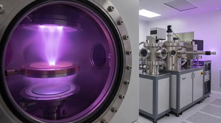
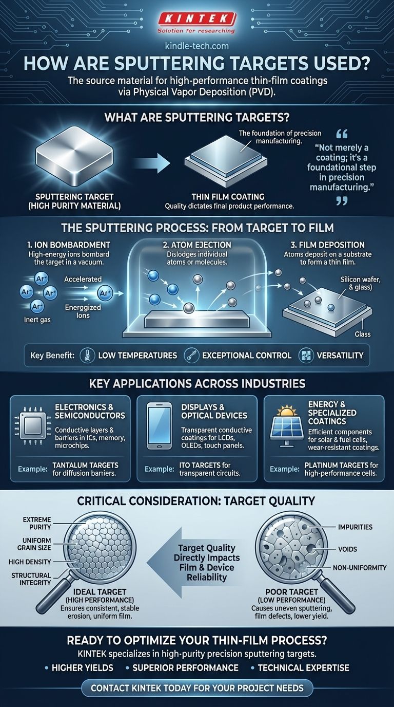
In short, sputtering targets are the source material used in a physical vapor deposition process called "sputtering" to create extremely thin, high-performance coatings. In this process, the target—a block of highly pure material—is bombarded with energized ions in a vacuum, which dislodges atoms that then deposit onto a substrate, such as a silicon wafer or piece of glass, to form a thin film.
The use of a sputtering target is not merely about applying a coating; it's a foundational step in precision manufacturing. The quality and composition of the target directly dictate the performance, purity, and reliability of the final product, from a microchip to a solar panel.
What is Sputtering? A High-Level Overview
Sputtering is a method for creating films of material that can be just a few nanometers thick. It's a cornerstone of modern manufacturing due to its control and versatility.
The Core Mechanism: From Target to Film
The process takes place within a vacuum chamber. High-energy ions, typically from an inert gas like argon, are accelerated and directed at the sputtering target.
This bombardment acts like a microscopic sandblaster, knocking individual atoms or molecules off the surface of the target. These ejected particles travel through the vacuum and land on a substrate, gradually building up to form a thin, uniform film.
Why Sputtering is Often Preferred
A key advantage of sputtering is its ability to operate at very low temperatures. This makes it ideal for depositing materials onto sensitive substrates that would be damaged by high-heat processes. It offers exceptional control over the thickness and composition of the deposited film.
Key Applications Across Major Industries
Sputtering targets are indispensable in any field that relies on high-performance thin films. The application dictates the specific material used for the target.
Electronics and Semiconductors
This is the largest application area. Sputtering is used to create the microscopic conductive layers and barriers within integrated circuits, memory chips, and microchips.
Tantalum targets, for example, are commonly used to create diffusion barriers that prevent different materials within the chip from mixing and causing failure.
Displays and Optical Devices
Transparent conductive coatings are essential for displays. Indium Tin Oxide (ITO) targets are sputtered to create the transparent circuits in LCDs, OLEDs, touch panels, and plasma displays.
ITO is also used for infrared-reflecting coatings on architectural and automotive glass, enhancing energy efficiency.
Energy and Specialized Coatings
The energy sector relies on sputtering for creating efficient components. Platinum targets are used in the manufacturing of high-performance solar cells and fuel cells.
Beyond energy, sputtering is used to apply hard, wear-resistant coatings to tools and components, as well as for high-end decorative finishes.
The Critical Consideration: Target Quality Dictates Results
A sputtering target is not simply a block of raw material. It is a highly engineered component where properties are controlled to an exacting degree. The final film can only be as good as the target it came from.
More Than Just Purity
While extremely high purity is the most basic requirement, it's only the beginning. Target specifications also include precise control over density, grain size, and overall structural uniformity.
Any impurity or defect within the target, such as an oxide inclusion or a void, can be transferred to the thin film. This creates a point of failure that can compromise the entire device.
The Link Between Target and Performance
The physical structure of the target directly impacts the sputtering process itself. A uniform grain size and high density ensure a consistent and stable erosion rate, leading to a more uniform and predictable thin film.
Non-uniformity in the target can cause uneven sputtering, leading to defects in the film, lower manufacturing yields, and poor device performance. This is why target fabrication is a highly specialized field.
Making the Right Choice for Your Goal
Understanding the role of the target helps frame your manufacturing and material selection strategy.
- If your primary focus is high-volume electronics: The purity and defect control of your Tantalum or other metallic targets are directly linked to device yield and long-term reliability.
- If your primary focus is displays or optics: The compositional and structural uniformity of your ITO target will determine the transparency, conductivity, and overall quality of your final coating.
- If your primary focus is next-generation energy: The density and purity of your Platinum target are critical for maximizing the efficiency and lifespan of your solar or fuel cells.
Ultimately, the sputtering target is the genesis of the thin film, and its quality is the single most important factor in achieving a successful outcome.
Summary Table:
| Key Aspect | Description |
|---|---|
| Primary Function | Source material for Physical Vapor Deposition (PVD) to create thin films. |
| Core Mechanism | Bombarded by ions in a vacuum, ejecting atoms that coat a substrate. |
| Key Industries | Semiconductors, Displays (LCD/OLED), Solar Cells, Optical Coatings. |
| Critical Factors | Extreme Purity, Uniform Grain Size, High Density, Structural Integrity. |
| Common Materials | Tantalum (semiconductors), ITO (displays), Platinum (energy devices). |
Ready to Optimize Your Thin-Film Process?
The quality of your sputtering target is the foundation of your coating's performance. KINTEK specializes in high-purity lab equipment and consumables, including precision sputtering targets for semiconductor, display, and energy research and manufacturing.
We help you achieve:
- Higher Yields: Minimize film defects with targets of exceptional purity and uniformity.
- Superior Performance: Ensure the reliability and efficiency of your final products.
- Technical Expertise: Get support in selecting the right target material and specifications for your specific application.
Don't let target quality be the weak link in your manufacturing chain. Contact KINTEK today to discuss your project needs and discover how our solutions can enhance your results.
Visual Guide
Related Products
- Reference Electrode Calomel Silver Chloride Mercury Sulfate for Laboratory Use
- Multifunctional Electrolytic Electrochemical Cell Water Bath Single Layer Double Layer
- Molybdenum Tungsten Tantalum Special Shape Evaporation Boat
- Hemispherical Bottom Tungsten Molybdenum Evaporation Boat
- Cylindrical Press Mold with Scale for Lab
People Also Ask
- Why is the selection of a high-quality reference electrode critical in the electrochemical synthesis? | KINTEK
- Which type of electrode can be used as a reference point? Select the Right One for Accurate Measurements
- How does the selection of reference electrodes correlate with electrolyte pH in HER testing? Ensure Precise Potential
- What is the function of a reference electrode? Master Precision in Three-Electrode Reactor Reconstruction
- What is the reference electrode in potentiometry? The Key to Stable & Accurate Measurements


