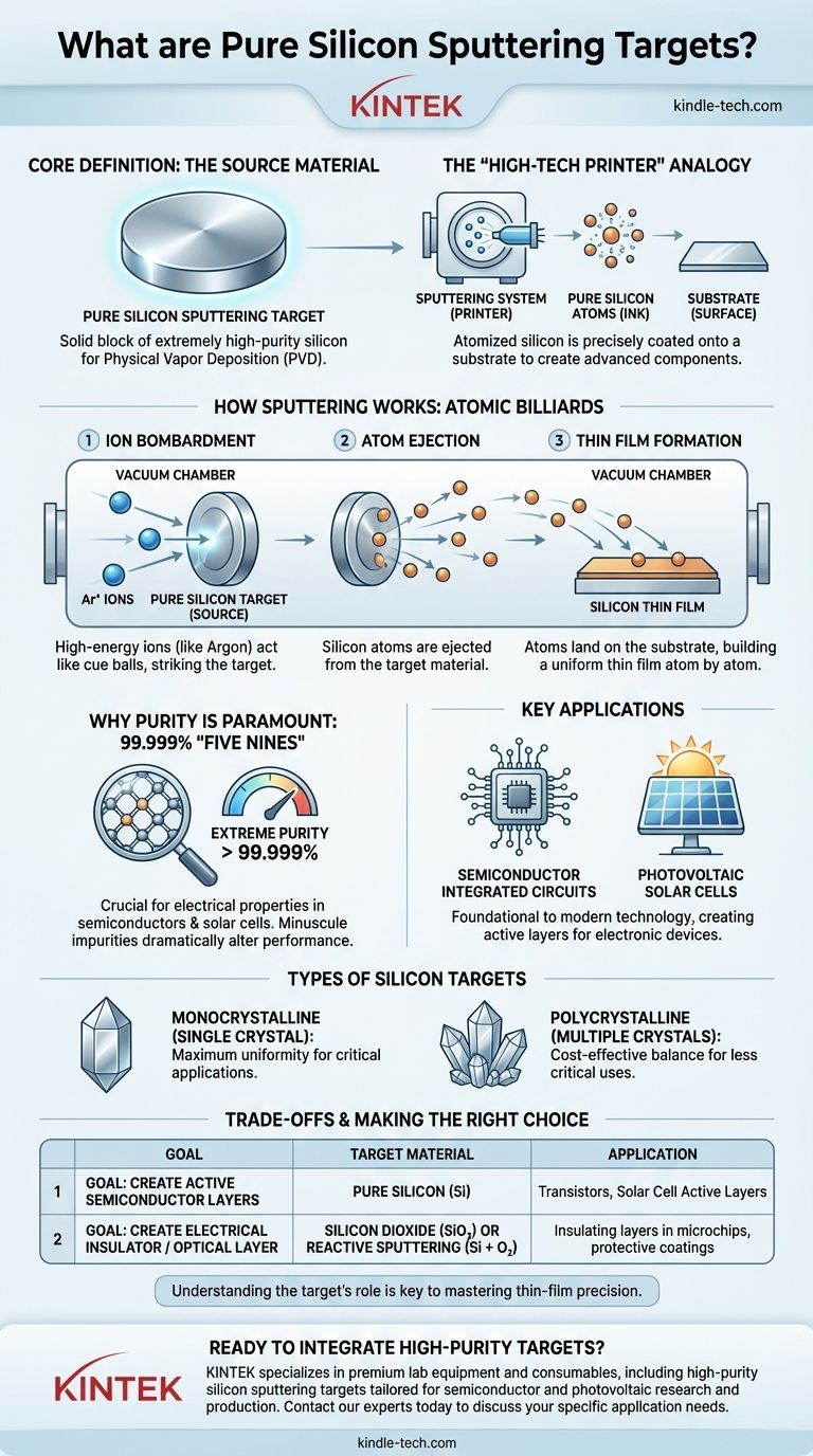
At its core, a pure silicon sputtering target is a solid block or disk of extremely high-purity silicon. It serves as the source material in a physical vapor deposition (PVD) process known as sputtering, which is used to deposit an ultra-thin, uniform layer of silicon onto a surface, or substrate.
The central concept to grasp is that a sputtering target acts like a solid source of ink for a high-tech printer. The "printer" is the sputtering system, and the "ink" is the pure silicon, which is atomized and precisely coated onto a material to create advanced electronic or optical components.
What is Sputtering? A Foundational Analogy
The Sputtering Process Explained
Imagine a high-energy game of atomic billiards. In a vacuum chamber, you fire high-energy ions (typically of an inert gas like argon) at the sputtering target. These ions act like a cue ball, striking the target with enough force to knock loose individual atoms or molecules.
The Role of the Target
The sputtering target is the rack of balls in our analogy—it is the source material you wish to deposit. In this case, the target is a solid piece of pure silicon. When struck by the ions, it ejects silicon atoms.
The Formation of a Thin Film
These ejected silicon atoms travel through the vacuum and land on a nearby object, known as the substrate. They gradually build up, atom by atom, to form a perfectly uniform and controlled thin film of silicon on the substrate's surface.
The Significance of "Pure Silicon"
Why Purity is Paramount
In applications like semiconductors and solar cells, the electrical properties of the silicon film are critical. Even minuscule amounts of impurities—measured in parts per million or even parts per billion—can dramatically alter performance or render a device useless.
For this reason, silicon targets are manufactured to extreme purity levels, often described as "five nines" (99.999%) or higher.
Key Applications of Silicon Films
Films deposited from pure silicon targets are foundational to modern technology. They are primarily used to create the active layers in devices where silicon's unique semiconducting properties are essential.
The most common applications include the fabrication of semiconductor integrated circuits (microchips) and the production of photovoltaic solar cells.
Monocrystalline vs. Polycrystalline Targets
Silicon targets come in two main forms. Monocrystalline targets are cut from a single, perfect silicon crystal, ensuring maximum uniformity in the deposited film.
Polycrystalline targets are formed from many smaller silicon crystals. They are generally less expensive but can result in a slightly less uniform film structure, making them suitable for less critical applications.
Understanding the Trade-offs: Pure Silicon vs. Silicon Compounds
A common point of confusion is choosing between a pure silicon target and a target made from a silicon compound, like silicon dioxide. The choice depends entirely on the desired property of the final film.
When to Use Pure Silicon (Si)
Use a pure silicon target when you need to deposit a film of elemental silicon. This is required for creating the active, current-carrying layers in transistors or the light-absorbing layers in solar cells.
When to Use Silicon Dioxide (SiO₂)
Use a silicon dioxide (SiO₂) target, also known as fused quartz, when your goal is to create a film that is an electrical insulator or a protective optical coating. SiO₂ is hard, transparent, and does not conduct electricity, making it ideal for insulating different layers of a microchip from each other.
An Advanced Technique: Reactive Sputtering
It is also possible to create a silicon dioxide film using a pure silicon target. This is done through a process called reactive sputtering, where a reactive gas like oxygen is introduced into the vacuum chamber along with the argon. The ejected silicon atoms react with the oxygen on their way to the substrate, forming a silicon dioxide film.
Making the Right Choice for Your Application
Choosing the correct target material is the first decision in designing a thin-film deposition process. Your choice is dictated by the function of the final layer you intend to create.
- If your primary focus is creating active semiconductor layers: You must use a high-purity, often monocrystalline, silicon target to achieve the required electronic properties.
- If your primary focus is creating an electrical insulator or a transparent protective layer: A silicon dioxide (SiO₂) target is the most direct choice, or you can use reactive sputtering with a pure silicon target and oxygen.
- If your primary focus is cost-sensitive R&D or non-critical applications: A polycrystalline silicon target can offer a practical balance of performance and budget.
Understanding the specific role of the target material is the first step toward mastering the precision of thin-film deposition.
Summary Table:
| Feature | Description |
|---|---|
| Material | Solid block/disk of extremely high-purity silicon (e.g., 99.999%). |
| Primary Use | Source material for sputtering, a Physical Vapor Deposition (PVD) process. |
| Key Applications | Semiconductor integrated circuits (microchips), photovoltaic solar cells. |
| Common Types | Monocrystalline (single crystal) and Polycrystalline (multiple crystals). |
| Alternative | Silicon Dioxide (SiO₂) targets for creating insulating or optical layers. |
Ready to integrate high-purity sputtering targets into your lab's workflow?
KINTEK specializes in providing premium lab equipment and consumables, including high-purity silicon sputtering targets tailored for semiconductor and photovoltaic research and production. Our expertise ensures you get the right materials for precise thin-film deposition, enhancing your device performance and yield.
Contact our experts today to discuss your specific application needs and discover how KINTEK can support your laboratory's success.
Visual Guide
Related Products
- Silicon Carbide (SIC) Ceramic Sheet Wear-Resistant Engineering Advanced Fine Ceramics
- Laboratory CVD Boron Doped Diamond Materials
- Optical Window Glass Substrate Wafer Quartz Plate JGS1 JGS2 JGS3
- Silicon Carbide (SIC) Ceramic Sheet Flat Corrugated Heat Sink for Engineering Advanced Fine Ceramics
- Precision Machined Silicon Nitride (SiN) Ceramic Sheet for Engineering Advanced Fine Ceramics
People Also Ask
- What are the common uses of silicon carbide? Unlock Extreme Performance in Harsh Environments
- What is the type of silicon carbide? A Guide to Polymorphs, Grades, and Applications
- What is the process of making silicon carbide? From Raw Materials to Advanced Ceramics
- What are the uses of silicon carbide ceramics in different industries? Master Extreme Performance in Aerospace, Semiconductors & More
- Why is silicon carbide more efficient? Unlock Higher Power Density with SiC's Superior Material Properties


