In essence, sputter targets are highly pure source materials used to create ultra-thin films on a substrate. This process, known as sputter deposition, is the foundation for manufacturing many of the high-tech components we rely on daily, from the microchips in your phone to the anti-reflective coating on your glasses.
The core purpose of a sputter target is not simply to coat a surface. It is to enable the precision engineering of materials at the atomic level, creating thin, uniform films with specific properties that are essential for modern electronics, optics, and advanced material science.

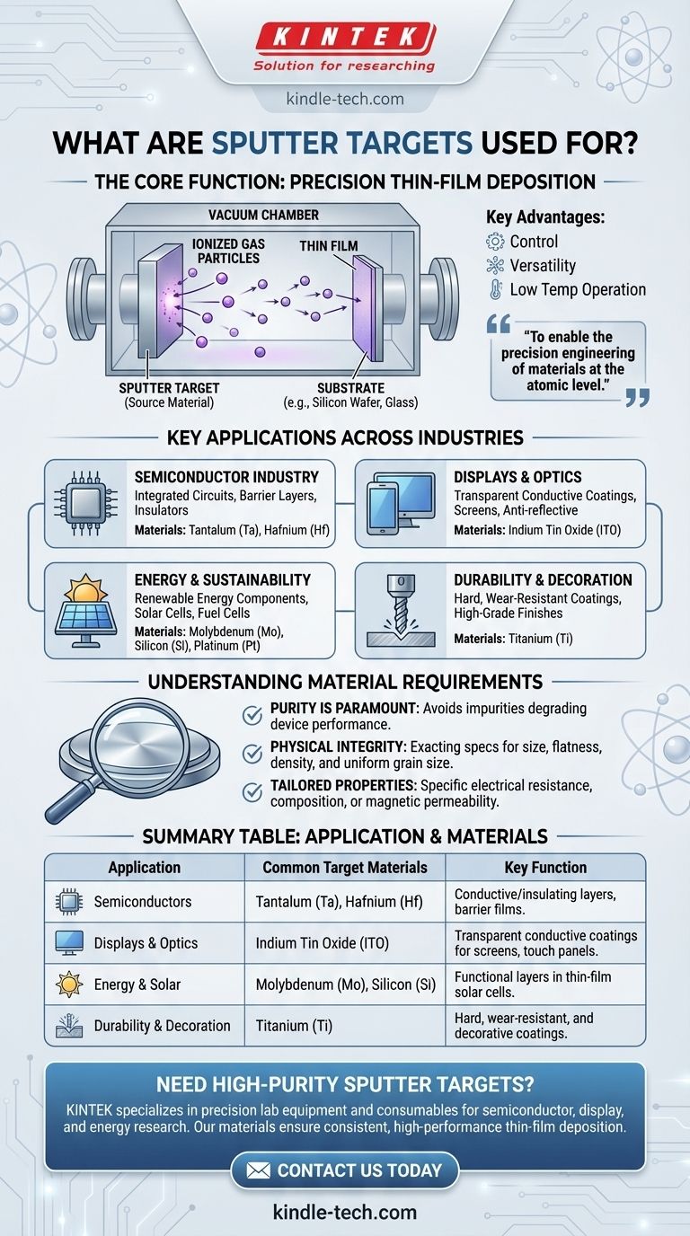
The Core Function: Precision Thin-Film Deposition
Sputtering is a physical vapor deposition (PVD) method. It involves bombarding a sputter target (the source material) with energized ions in a vacuum, which dislodges or "sputters" atoms from the target. These atoms then travel and deposit onto a substrate (like a silicon wafer or glass panel), forming an extremely thin and uniform film.
Why Sputtering is a Critical Process
The primary advantage of sputtering is its control and versatility. The process can operate at very low temperatures, which is crucial for protecting sensitive substrates like electronic components.
It allows for the deposition of a vast range of materials, including metals, alloys, and ceramics, enabling the creation of complex, multi-layered structures with highly specific functions.
Key Applications Across Industries
The unique capabilities of sputter deposition mean its applications are widespread, particularly in industries that demand high performance and miniaturization.
In the Semiconductor Industry
This is arguably the largest application. Sputter targets are used to deposit the microscopic layers of conductive and insulating materials that form integrated circuits.
For example, Tantalum (Ta) targets are used to create critical barrier layers on silicon wafers, preventing materials from mixing and ensuring the reliability of microchips, memory chips, and print heads. Hafnium (Hf) is often used as a high-performance insulator.
For Displays and Optics
Sputtering is essential for creating the transparent conductive coatings on modern screens.
Indium Tin Oxide (ITO) targets are the industry standard for making these coatings on LCDs, flat-panel displays, touch panels, and even solar cells. Other applications include infrared-reflecting coatings for automotive glass.
In Energy and Sustainability
The process is vital for manufacturing renewable energy components.
Molybdenum (Mo) and Silicon (Si) targets are used to deposit the functional layers within thin-film solar panel cells. Platinum (Pt) targets are critical for applications in both solar cells and advanced fuel cells.
For Durability and Decoration
Sputtering can create surfaces with enhanced physical properties.
Titanium (Ti) is used for its light weight and corrosion resistance, creating hard, wear-resistant coatings for tools and components. It is also used to apply high-grade decorative finishes.
Understanding the Material Requirements
Sputter targets are not simply blocks of raw material. They are highly engineered components with far stricter requirements than materials used in traditional industries. The performance of the final thin film is directly dependent on the quality of the target.
Purity is Paramount
The purity of the target material is one of the most critical factors. Even minute impurities in the target can get incorporated into the thin film, severely degrading the performance of a semiconductor or optical device.
Physical and Structural Integrity
Targets must meet exacting specifications for size, flatness, and density. Internal characteristics like grain size uniformity and the absence of defects are tightly controlled to ensure a consistent and predictable sputtering rate.
Tailored Properties
Depending on the application, targets must have specific properties, such as a desired electrical resistance, composition uniformity, or magnetic permeability. These are not bulk materials; they are precision-engineered components.
How Sputtering Targets Enable Specific Goals
Your choice of sputter target material is dictated entirely by the function you need the thin film to perform.
- If your primary focus is creating advanced electronics: You will rely on materials like Tantalum and Hafnium to build the microscopic conductive and insulating layers in integrated circuits.
- If your primary focus is developing transparent conductive surfaces: Indium Tin Oxide (ITO) targets are the industry standard for creating the functional coatings on displays, touch panels, and solar cells.
- If your primary focus is enhancing surface durability or energy efficiency: Materials like Titanium (for hardness) and Molybdenum (for solar cells) are used to create high-performance functional coatings.
Ultimately, sputter targets are the foundational source materials that make the performance and miniaturization of modern high technology possible.
Summary Table:
| Application | Common Target Materials | Key Function |
|---|---|---|
| Semiconductors | Tantalum (Ta), Hafnium (Hf) | Conductive/insulating layers, barrier films |
| Displays & Optics | Indium Tin Oxide (ITO) | Transparent conductive coatings for screens, touch panels |
| Energy & Solar | Molybdenum (Mo), Silicon (Si) | Functional layers in thin-film solar cells |
| Durability & Decoration | Titanium (Ti) | Hard, wear-resistant, and decorative coatings |
Need high-purity sputter targets tailored to your application? KINTEK specializes in precision lab equipment and consumables, including sputter targets for semiconductor, display, and energy research. Our materials ensure consistent, high-performance thin-film deposition. Contact us today to discuss your specific requirements and enhance your lab's capabilities!
Visual Guide
Related Products
- Multifunctional Electrolytic Electrochemical Cell Water Bath Single Layer Double Layer
- Reference Electrode Calomel Silver Chloride Mercury Sulfate for Laboratory Use
- Laboratory CVD Boron Doped Diamond Materials
- Square Lab Press Mold for Laboratory Applications
- Electron Beam Evaporation Coating Oxygen-Free Copper Crucible and Evaporation Boat
People Also Ask
- What are the typical volumes and aperture configurations for a double-layer water-bath electrolytic cell? Optimize Your Electrochemical Setup
- What is the typical volume range of the multifunctional electrolytic cell? Choosing the Right Size for Your Lab
- What is the typical experimental system used with a double-layer water-bath electrolytic cell? Achieve Precise Electrochemical Control
- How can water and gas leaks be prevented in a double-layer water-bath electrolytic cell? A Guide to Proactive Maintenance
- What are the procedures for after using a double-layer water-bath electrolytic cell? Ensure Equipment Longevity and Data Accuracy


