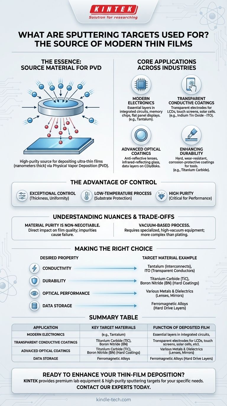
In essence, sputtering targets are the source material used in a high-vacuum process to deposit ultra-thin films onto the surface of another object, known as a substrate. These films, often only a few nanometers thick, are fundamental to manufacturing a vast range of modern products, from microchips and displays to protective coatings on cutting tools.
The core function of a sputtering target is to serve as a high-purity source for creating precisely controlled thin-film coatings. This process, called sputter deposition, is not just one application among many—it is the foundational manufacturing technique that enables the advanced functionality of countless electronic, optical, and mechanical components.
The Foundation: How Sputter Deposition Works
To understand what sputtering targets are used for, you must first understand the process they enable. The target is not the end product; it is the starting point for a sophisticated deposition method.
A High-Vacuum Process
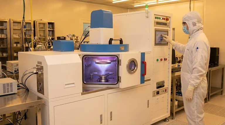
Sputtering is a form of Physical Vapor Deposition (PVD). Inside a vacuum chamber, the sputtering target is bombarded with high-energy ions, which physically knock atoms loose from the target's surface.
From Target to Thin Film
These ejected atoms travel through the vacuum and land on a substrate, such as a silicon wafer or a piece of glass. They gradually build up on the substrate, forming a dense, uniform, and extremely thin film.
The Advantage of Control
The sputtering process allows for exceptional control over film thickness, uniformity, and composition. It can also be performed at very low temperatures, making it ideal for coating sensitive materials that would be damaged by other high-heat methods.
Core Applications Across Industries
The ability to create these precise thin films means sputtering targets are used in nearly every high-tech industry. The applications are defined by the properties of the film being deposited.
The Heart of Modern Electronics
This is the largest and most critical application. Thin films created from sputtering targets form the essential layers of microelectronic components.
Examples include the conductive pathways in integrated circuits (microchips), the data storage layers in memory chips, and the complex circuitry in flat panel displays. Targets made of materials like Tantalum are common for these uses.
Transparent Conductive Coatings
A specialized but vital electronic application is the creation of transparent films that also conduct electricity.
Indium Tin Oxide (ITO) targets are sputtered onto glass or plastic to create the transparent electrodes essential for LCDs, touch screens, and plasma displays. These ITO films are also used in solar cells and for antistatic coatings.
Advanced Optical Coatings
Sputtering is used to precisely alter the way light interacts with a surface.
This includes creating infrared-reflecting coatings for automotive glass, anti-reflective layers for lenses, and the reflective data layers on CDs and disk drives.
Enhancing Durability and Performance
Thin films can also serve a protective purpose, dramatically increasing the lifespan and performance of tools and components.
Hard coatings from targets like Titanium Carbide (TiC) are applied to cutting tools to make them incredibly wear-resistant. Other films provide corrosion protection or act as solid lubricants in high-friction environments.
Understanding the Nuances and Trade-offs
While powerful, sputter deposition is a complex process with specific requirements that dictate its use. Understanding these trade-offs is key to appreciating its role.
Material Purity is Non-Negotiable
The quality of the final thin film is directly dependent on the purity of the sputtering target. Any impurity in the target material can be transferred to the film, potentially causing a catastrophic failure in a microchip or optical lens.
It Is a Vacuum-Based Process
Sputtering requires highly specialized and expensive equipment, including a high-vacuum chamber. This makes it a more complex and costly process than simple plating or wet chemical coating methods.
More Than Just Deposition
While deposition is its primary use, the sputtering phenomenon is also leveraged for other high-tech purposes. It can be used for ultra-fine surface cleaning to prepare a substrate for other processes or for surface analysis to determine the chemical composition of a material.
Making the Right Choice for Your Goal
The selection of a sputtering target is dictated entirely by the desired properties of the final thin film. The material of the target defines the function of the coating.
- If your primary focus is conductivity: Materials like Tantalum are used for circuit interconnects, while Indium Tin Oxide (ITO) is the standard for transparent conductors in displays.
- If your primary focus is durability: Ceramic targets such as Titanium Carbide (TiC) or Boron Nitride (BN) are chosen to create hard, wear-resistant protective coatings.
- If your primary focus is optical performance: A wide range of metal and dielectric targets are used to create films with specific refractive or reflective properties for lenses, mirrors, and solar cells.
- If your primary focus is data storage: Ferromagnetic alloys are sputtered to create the magnetic layers that store data on hard disk drives and other memory devices.
Ultimately, sputtering targets are the invisible but essential source material upon which much of modern technological hardware is built.
Summary Table:
| Application | Key Target Materials | Function of Deposited Film |
|---|---|---|
| Microelectronics & Integrated Circuits | Tantalum, Copper, Aluminum | Conductive pathways, data storage layers |
| Transparent Conductive Coatings (Displays, Touch Screens) | Indium Tin Oxide (ITO) | Transparent electrodes, anti-static layers |
| Hard & Wear-Resistant Coatings | Titanium Carbide (TiC), Boron Nitride (BN) | Protective layers for cutting tools, components |
| Optical Coatings (Lenses, Solar Cells) | Various metals, dielectrics | Anti-reflective, infrared-reflecting layers |
| Data Storage (Hard Drives, Memory) | Ferromagnetic alloys | Magnetic data storage layers |
Ready to enhance your thin-film deposition process with high-purity sputtering targets?
KINTEK specializes in providing premium lab equipment and consumables, including sputtering targets tailored for your specific application—whether in microelectronics, optics, or protective coatings. Our targets ensure the material purity and performance required for reliable, high-quality thin films.
Contact our experts today to discuss your project needs and discover how KINTEK can support your laboratory's success with precision-engineered solutions.
Visual Guide
Related Products
- Reference Electrode Calomel Silver Chloride Mercury Sulfate for Laboratory Use
- Cylindrical Press Mold with Scale for Lab
- Laboratory CVD Boron Doped Diamond Materials
- Molybdenum Tungsten Tantalum Special Shape Evaporation Boat
- Multifunctional Electrolytic Electrochemical Cell Water Bath Single Layer Double Layer
People Also Ask
- Which electrode is used as a ground reference? Master the Key to Accurate Electrochemical Measurements
- Why is the selection of a high-quality reference electrode critical in the electrochemical synthesis? | KINTEK
- Which type of electrode can be used as a reference point? Select the Right One for Accurate Measurements
- How does the selection of reference electrodes correlate with electrolyte pH in HER testing? Ensure Precise Potential
- Which electrode is used as a reference? A Guide to Accurate Electrochemical Measurements