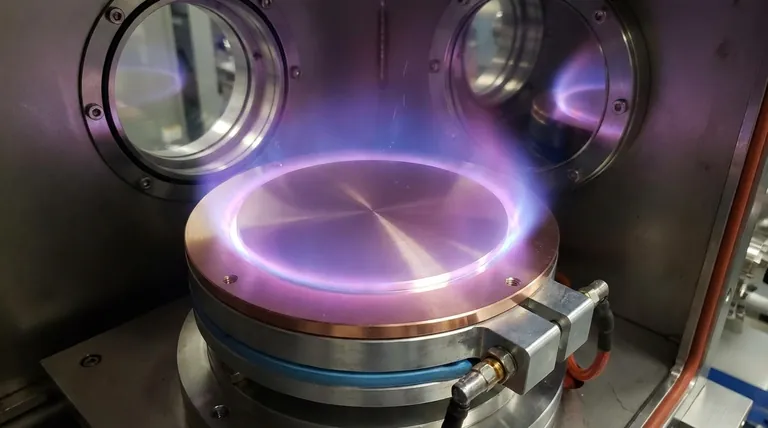
A sputtering target's specifications are a comprehensive set of material, physical, and geometric properties that define its quality and performance. These include critical metrics like material purity, density, grain size, and dimensional tolerance, which are far more stringent than those for standard bulk materials because they directly control the quality and consistency of the final deposited thin film.
The core principle is that a sputtering target is not merely a source material; it is a precision component. Its specifications must be carefully matched to the deposition system and the functional requirements of the thin film being created, as each property directly influences the sputtering rate, film purity, and process stability.
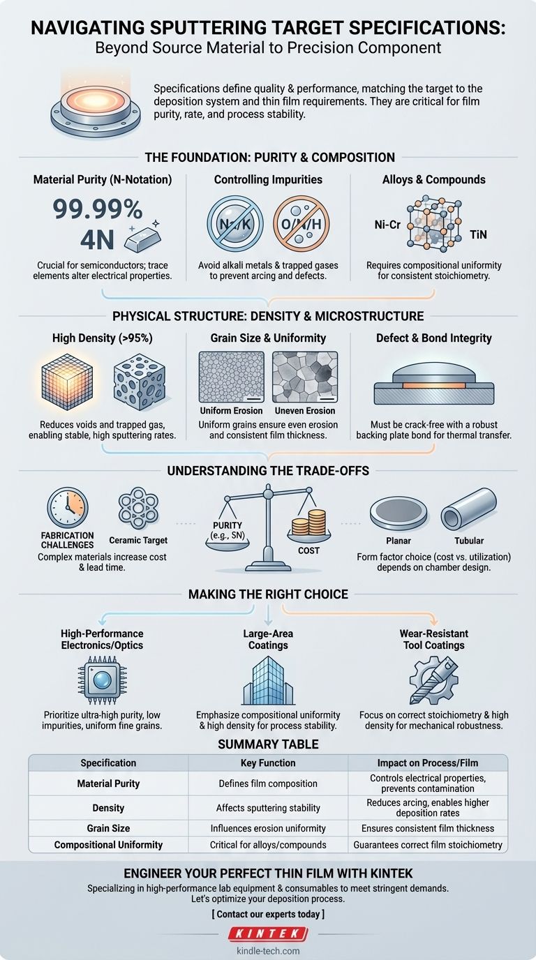
The Foundation: Purity and Composition
The chemical makeup of the target is the most fundamental aspect, as it is what ultimately forms your film.
Defining Material Purity
The purity of the target material is paramount. It is typically expressed as a percentage (e.g., 99.99%) or using "N" notation (e.g., 4N for 99.99%, 5N for 99.999%).
High purity is essential for applications like semiconductors and electronics, where even trace amounts of an unwanted element can drastically alter the film's electrical properties and render a device useless.
Controlling Specific Impurities
Beyond overall purity, the type and concentration of specific impurities are critical. For example, alkali metal impurities (Na, K) are highly detrimental in semiconductor manufacturing.
Gaseous impurities like oxygen, nitrogen, and hydrogen trapped within the target are also a major concern, as they can cause arcing during sputtering or become incorporated into the film, creating defects.
Alloys and Compounds
Many applications use targets that are not pure elements but precise alloys (e.g., Nickel-Chromium) or compounds (e.g., Titanium Nitride, Indium Tin Oxide).
For these materials, the key specification becomes compositional uniformity. The elements must be homogeneously mixed throughout the target to ensure the deposited film has a consistent and correct stoichiometry from start to finish.
Physical Structure: Density and Microstructure
The internal physical structure of the target has a direct impact on the stability and efficiency of the sputtering process itself.
The Importance of High Density
Density, measured as a percentage of the material's theoretical maximum density, is a key performance indicator. High-density targets (typically >95%) are crucial.
Low density implies the presence of internal voids. These voids can trap gas, leading to uncontrolled gas release and arcing during the process. A denser target also allows for a higher, more stable sputtering rate.
Grain Size and Uniformity
For metallic and alloy targets, a small and uniform grain size is highly desirable. Large or non-uniform grains will sputter at different rates, leading to uneven erosion of the target surface.
This uneven erosion translates directly into poor thickness uniformity in the deposited film. Therefore, controlling the target's microstructure is essential for creating consistent coatings.
Defect and Bond Integrity
The target must be free of cracks, inclusions, or other physical defects. These act as points of failure and can generate particles that contaminate the substrate.
Furthermore, the target material is typically bonded to a metallic "backing plate," which provides mechanical support and facilitates water cooling. The integrity of this bond is critical for efficient thermal transfer to prevent the target from overheating and cracking.
Understanding the Trade-offs
Choosing the right specifications is an exercise in balancing performance requirements with practical constraints.
Purity vs. Cost
The single biggest trade-off is purity versus cost. Each additional "nine" in purity (e.g., moving from 4N to 5N) can increase the price significantly due to the complex refining processes required.
For applications like architectural glass, a 3N target may be perfectly sufficient, whereas for advanced microelectronics, 5N or 6N purity is non-negotiable. Over-specifying purity is a common and costly mistake.
Fabrication Challenges
Some materials, particularly ceramics and brittle intermetallic compounds, are notoriously difficult to fabricate into high-density, defect-free targets.
This manufacturing complexity directly impacts cost and lead time. A simple aluminum target may be readily available, while a large, crack-free ceramic target might require a specialized manufacturing process and a lead time of several weeks or months.
Form Factor and Utilization
Targets come in various shapes, most commonly planar (flat/rectangular) and tubular (cylindrical). Planar targets are often simpler and cheaper to manufacture.
However, tubular targets, used in certain large-area coating systems, can offer much higher material utilization, reducing the cost per substrate over the target's lifetime. The choice is dictated by the design of your sputtering chamber.
Making the Right Choice for Your Application
Ultimately, the target specifications you require are defined by your end goal.
- If your primary focus is high-performance electronics or optics: Prioritize ultra-high purity, extremely low specific impurities, and a uniform, fine-grain microstructure to ensure predictable film properties.
- If your primary focus is large-area protective or architectural coatings: Emphasize compositional uniformity and high density for process stability, but select a purity grade and form factor that provides the best cost-effectiveness for your operation.
- If your primary focus is wear-resistant tool coatings: Concentrate on achieving the correct stoichiometry in compound targets and ensuring high density to produce a mechanically robust film free of defects.
Mastering these specifications transforms the sputtering target from a simple consumable into a precision instrument for engineering your desired film.
Summary Table:
| Specification | Key Function | Impact on Process/Film |
|---|---|---|
| Material Purity | Defines film composition | Controls electrical properties, prevents contamination |
| Density | Affects sputtering stability | Reduces arcing, enables higher deposition rates |
| Grain Size | Influences erosion uniformity | Ensures consistent film thickness |
| Compositional Uniformity | Critical for alloys/compounds | Guarantees correct film stoichiometry |
Engineer Your Perfect Thin Film with KINTEK
Choosing the right sputtering target specifications is critical for your lab's success. Whether you are developing advanced semiconductors, high-performance optics, or durable protective coatings, the precise purity, density, and microstructure of your target define your results.
KINTEK specializes in high-performance lab equipment and consumables, providing sputtering targets engineered to meet the stringent demands of modern research and production. We help you navigate the trade-offs between purity, cost, and manufacturability to select the ideal target for your specific application, ensuring process stability and superior film quality.
Let's optimize your deposition process. Contact our experts today to discuss your project requirements and find the perfect sputtering solution.
Visual Guide
Related Products
- Reference Electrode Calomel Silver Chloride Mercury Sulfate for Laboratory Use
- Multifunctional Electrolytic Electrochemical Cell Water Bath Single Layer Double Layer
- Laboratory CVD Boron Doped Diamond Materials
- Cylindrical Press Mold with Scale for Lab
- Square Lab Press Mold for Laboratory Applications
People Also Ask
- What is the reference electrode in potentiometry? The Key to Stable & Accurate Measurements
- What is the recommended maintenance for the filling solution of a reference electrode? A Guide to Stable & Accurate Readings
- Which electrode is used as a reference electrode for measuring half-cell potentials? Understanding the Universal Standard
- What is the purpose of the reference electrode? Achieve Stable & Accurate Electrochemical Measurements
- Why is the selection of a high-quality reference electrode critical in the electrochemical synthesis? | KINTEK


