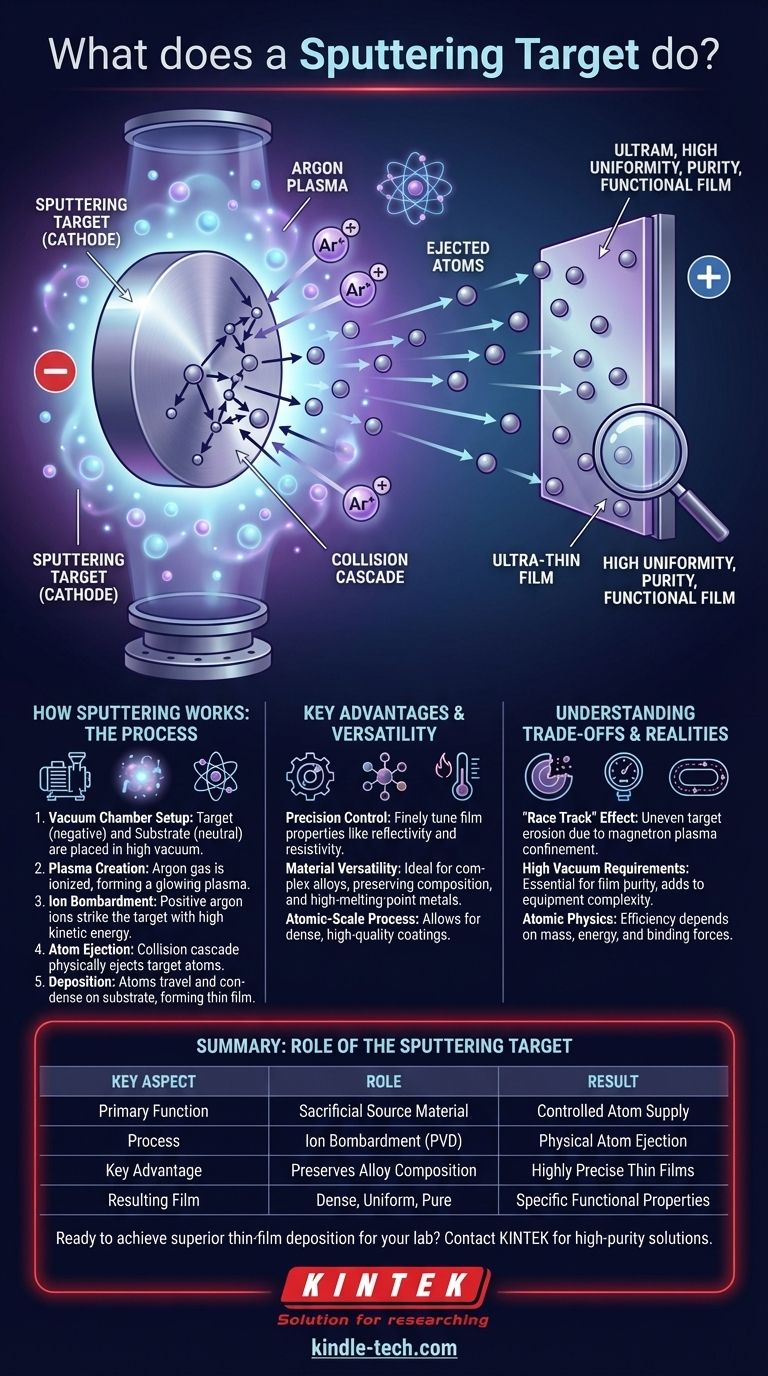
In any sputtering process, the sputtering target is the source material—a solid ingot or plate of the exact substance you intend to deposit as an ultra-thin film. Energetic ions in a vacuum chamber bombard this target, physically knocking atoms loose from its surface. These ejected atoms then travel and coat a nearby object, known as the substrate, forming the desired thin film.
The core challenge in advanced manufacturing and research is depositing highly uniform, pure, and functional thin films. The sputtering target solves this by acting as a high-purity, sacrificial source, providing a steady stream of atoms that can be precisely layered onto a surface in a highly controlled vacuum environment.
How Sputtering Works: The Target's Central Role
Sputtering is a type of Physical Vapor Deposition (PVD), meaning it transfers material physically, not chemically. The target is the absolute center of this physical process.
The Setup: Target, Substrate, and Vacuum
The entire process occurs inside a vacuum chamber. The sputtering target (the source material) is installed and given a negative electrical charge, making it the cathode.
The object to be coated, called the substrate, is placed nearby and typically acts as the anode (or is kept neutral).
Creating the Plasma
The chamber is filled with a small amount of an inert gas, almost always argon. A high voltage is applied, which ionizes this gas, stripping electrons from the argon atoms.
This process creates a plasma, a glowing cloud of positively charged argon ions and free electrons.
The Ion Bombardment
Because opposites attract, the positively charged argon ions are forcefully accelerated toward the negatively charged sputtering target.
These ions strike the target's surface with significant kinetic energy.
The "Collision Cascade" and Atom Ejection
The impact of an argon ion doesn't just chip off one atom. It sets off a collision cascade beneath the target's surface, similar to a multi-ball break shot in pool.
This transfer of momentum bounces through the material's atomic structure. When the energy from this cascade reaches the surface, it can overcome the surface binding energy, ejecting atoms of the target material into the vacuum chamber.
Deposition: From Target to Substrate
These newly freed atoms from the target travel in a straight line through the vacuum until they strike the substrate.
Upon hitting the substrate, they stick and begin to build up, nucleating and forming a dense, uniform, and high-purity thin film.
Why Sputtering (and the Target) Are So Important
Sputtering is a preferred method in many high-tech industries, from semiconductors to optics, because of the control it offers.
Precision Control Over Film Properties
Because sputtering is a fine, atom-by-atom process, it allows for extremely precise control over the final film's characteristics.
Engineers can finely tune properties like reflectivity, electrical resistivity, film density, and even the crystal grain structure of the coating.
Versatility with Materials
Sputtering is exceptionally useful for depositing materials that are otherwise difficult to work with. This includes alloys and metals with very high melting points.
Since the process physically ejects atoms rather than melting the bulk material, the composition of an alloy target is perfectly preserved in the final thin film.
Understanding the Trade-offs and Physical Realities
While powerful, the sputtering process has practical limitations and characteristics that are important to understand.
It's an Atomic-Scale Billiards Game
The efficiency of the process depends on physics—specifically, the mass of the sputtering gas ions (argon) relative to the target atoms, the ions' energy, and the target material's binding energy. Not every ion impact results in an ejected atom.
The "Race Track" Effect
A used sputtering target does not erode evenly. It typically develops a deep groove, often called a "race track," in the area of most intense ion bombardment.
This is because in modern systems (magnetron sputtering), magnets are used to trap the plasma close to the target's surface to increase sputtering efficiency, concentrating the ion impacts in a specific path.
High Vacuum Requirements
Sputtering demands a high-quality vacuum. Any residual gas molecules in the chamber can contaminate the vapor stream and compromise the purity of the thin film.
This requirement makes sputtering equipment more complex and costly than some alternative deposition methods.
Making the Right Choice for Your Goal
Understanding the target's function helps you decide if sputtering is the right method for your application.
- If your primary focus is depositing complex alloys or high-melting-point metals: Sputtering is a superior choice because it vaporizes material without altering its composition, a major challenge for evaporation-based methods.
- If your primary focus is achieving highly specific film properties (like density or optical performance): Sputtering offers exceptional control over the film's microstructure, resulting in high-quality, dense coatings.
- If your primary focus is cost-effective coating of simpler materials: You may want to evaluate other methods like thermal evaporation, which can be faster and require less complex equipment, though often with a trade-off in film quality.
Ultimately, understanding the sputtering target's role as the atomic source is the key to mastering precision thin-film deposition.
Summary Table:
| Key Aspect | Role of the Sputtering Target |
|---|---|
| Primary Function | Acts as the sacrificial source material for thin-film deposition |
| Process | Atoms are ejected via ion bombardment in a vacuum chamber |
| Key Advantage | Preserves exact composition of alloys and high-melting-point metals |
| Resulting Film | Highly uniform, dense, and pure coatings with precise properties |
Ready to achieve superior thin-film deposition for your lab?
At KINTEK, we specialize in high-purity sputtering targets and lab equipment tailored for advanced research and manufacturing. Whether you're working with complex alloys, high-melting-point metals, or need precise control over film properties, our solutions ensure consistent, reliable results.
Contact us today to discuss your specific application and discover how KINTEK can enhance your PVD processes with precision materials and expert support.
Visual Guide
Related Products
- Reference Electrode Calomel Silver Chloride Mercury Sulfate for Laboratory Use
- Multifunctional Electrolytic Electrochemical Cell Water Bath Single Layer Double Layer
- Molybdenum Tungsten Tantalum Special Shape Evaporation Boat
- Hemispherical Bottom Tungsten Molybdenum Evaporation Boat
- Cylindrical Press Mold with Scale for Lab
People Also Ask
- How does the selection of reference electrodes correlate with electrolyte pH in HER testing? Ensure Precise Potential
- Which electrode is used as a reference? A Guide to Accurate Electrochemical Measurements
- Why is the selection of a high-quality reference electrode critical in the electrochemical synthesis? | KINTEK
- What is the function of a reference electrode? Master Precision in Three-Electrode Reactor Reconstruction
- Which electrode is used as a ground reference? Master the Key to Accurate Electrochemical Measurements


