In the world of precision engineering and microfabrication, a gold sputtering target is the high-purity source material used to create an ultra-thin film of gold on another object, known as a substrate. This target, often a disc or plate of solid gold, is a critical component in a vacuum deposition process called sputtering, which transfers material atom by atom from the target to the substrate.
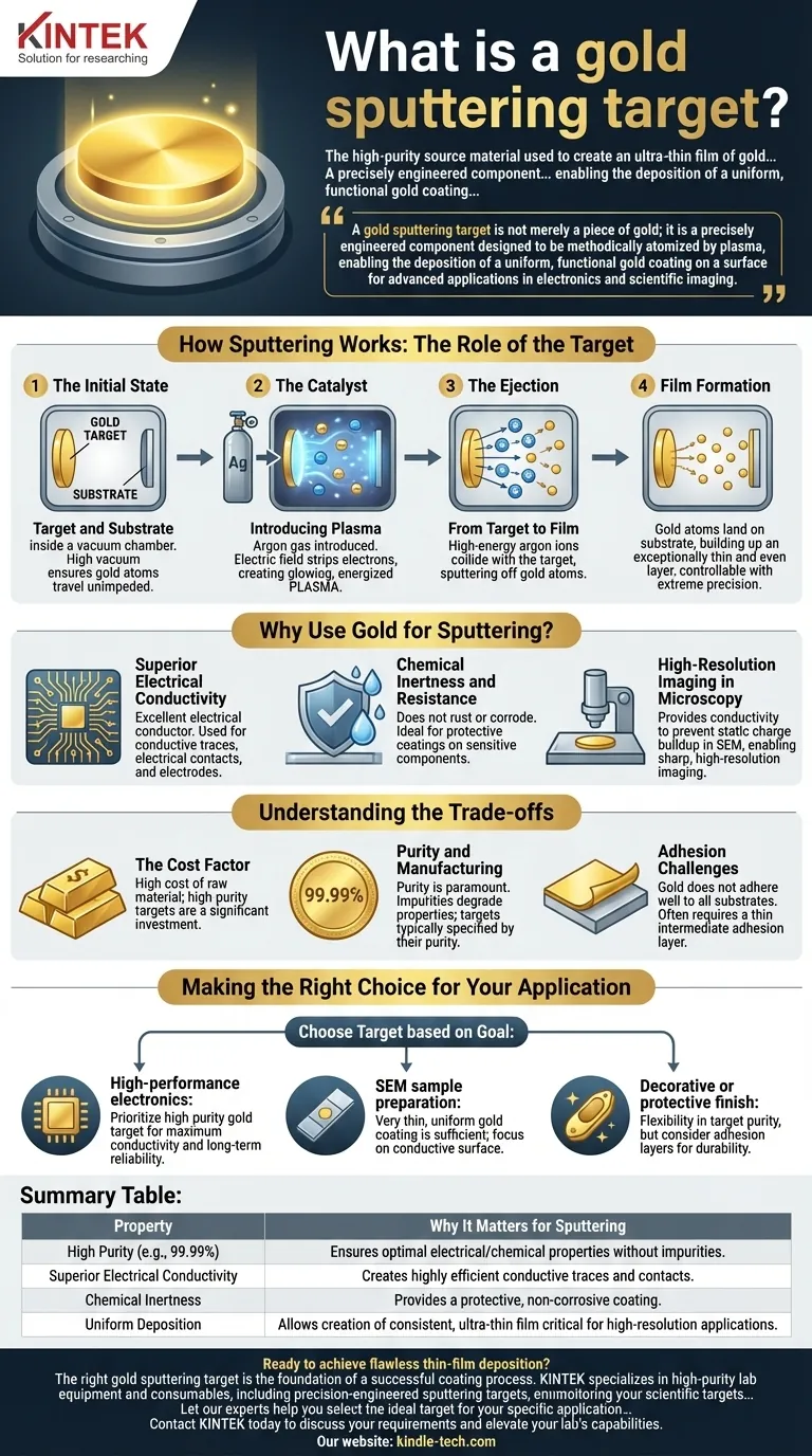
A gold sputtering target is not merely a piece of gold; it is a precisely engineered component designed to be methodically atomized by plasma, enabling the deposition of a uniform, functional gold coating on a surface for advanced applications in electronics and scientific imaging.
How Sputtering Works: The Role of the Target
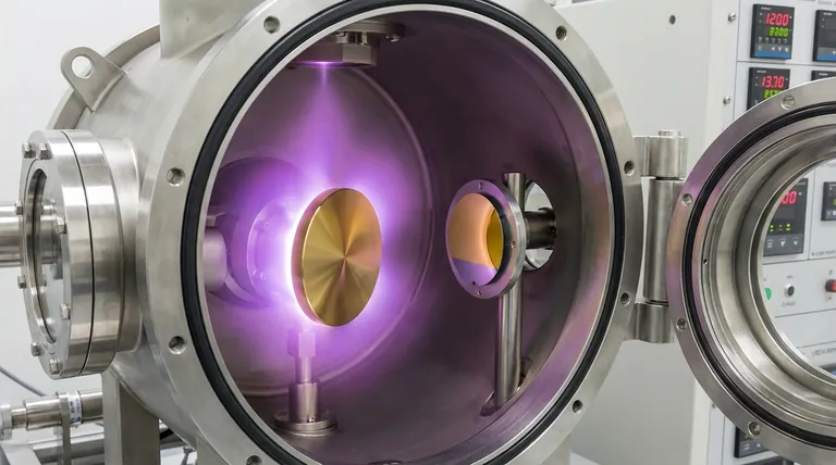
Sputtering is a type of Physical Vapor Deposition (PVD). The process can be understood as a controlled, atomic-scale sandblasting where the "sand" is a plasma of ionized gas and the "wall" being blasted is the gold target.
The Initial State: Target and Substrate
The process begins inside a vacuum chamber containing the gold target and the material to be coated, the substrate. A high vacuum is necessary to ensure the gold atoms can travel unimpeded.
The Catalyst: Introducing Plasma
An inert gas, typically argon, is introduced into the chamber. An electric field is applied, which strips electrons from the argon atoms, creating a glowing, energized state of matter known as plasma.
The Ejection: From Target to Film
The positively charged argon ions from the plasma are accelerated with high energy into the negatively charged gold target. This forceful collision knocks, or "sputters," individual gold atoms off the target's surface.
These ejected gold atoms then travel through the vacuum and land on the substrate, gradually building up an exceptionally thin and even layer. The thickness of this gold film can be controlled with extreme precision.
Why Use Gold for Sputtering?
Gold is chosen for specific technical advantages that justify its cost. The properties of the target material directly translate to the properties of the resulting thin film.
Superior Electrical Conductivity
Gold is an excellent electrical conductor. A thin sputtered layer of gold is often used to create conductive traces on circuit boards, electrical contacts, and electrodes in various electronic devices.
Chemical Inertness and Resistance
Gold does not rust or corrode. This chemical inertness makes it ideal for protective coatings on sensitive components that must operate reliably for long periods without degrading.
High-Resolution Imaging in Microscopy
In Scanning Electron Microscopy (SEM), non-conductive samples must be coated with a conductive layer to prevent the buildup of static charge, which would distort the image. A thin sputtered gold film provides this conductivity, enabling sharp, high-resolution imaging of biological or ceramic samples.
Understanding the Trade-offs
While powerful, gold sputtering has practical considerations that must be managed for successful application. Understanding these factors is key to achieving the desired outcome.
The Cost Factor
The most obvious trade-off is the high cost of the raw material. Gold is a precious metal, and high-purity targets required for demanding applications represent a significant investment.
Purity and Manufacturing
The purity of the target is paramount. Impurities in the gold target will be transferred to the thin film, potentially degrading its electrical or chemical properties. Targets are typically specified by their purity, such as "99.99%" (often called "four nines").
Adhesion Challenges
Gold does not naturally adhere well to all substrates, such as silicon wafers or glass. To overcome this, a very thin intermediate adhesion layer of a different metal, like titanium or chromium, is often sputtered onto the substrate first.
Making the Right Choice for Your Application
The decision to use a gold sputtering target depends entirely on your end goal. The process offers precision that is essential for certain high-value applications.
- If your primary focus is high-performance electronics: Prioritize a high-purity gold target to ensure maximum conductivity and long-term reliability for critical contacts and connections.
- If your primary focus is SEM sample preparation: A very thin, uniform gold coating is sufficient; the main goal is creating a conductive surface without obscuring the sample's features.
- If your primary focus is creating a decorative or protective finish: You may have more flexibility in target purity, but you must still consider adhesion layers to ensure the coating is durable.
Ultimately, viewing the sputtering target as the foundational source of your final surface's properties is the key to leveraging this powerful technology effectively.
Summary Table:
| Property | Why It Matters for Sputtering |
|---|---|
| High Purity (e.g., 99.99%) | Ensures the final coating has optimal electrical and chemical properties without impurities. |
| Superior Electrical Conductivity | Creates highly efficient conductive traces and contacts for electronic devices. |
| Chemical Inertness | Provides a protective, non-corrosive coating for sensitive components. |
| Uniform Deposition | Allows for the creation of a consistent, ultra-thin film critical for high-resolution applications. |
Ready to achieve flawless thin-film deposition?
The right gold sputtering target is the foundation of a successful coating process. KINTEK specializes in high-purity lab equipment and consumables, including precision-engineered sputtering targets designed for the demanding needs of electronics fabrication and scientific research.
Let our experts help you select the ideal target for your specific application. We provide the materials and support to ensure your projects in microfabrication and microscopy deliver superior performance and reliability.
Contact KINTEK today to discuss your requirements and elevate your lab's capabilities.
Visual Guide
Related Products
- Electron Beam Evaporation Coating Gold Plating Tungsten Molybdenum Crucible for Evaporation
- Hemispherical Bottom Tungsten Molybdenum Evaporation Boat
- Molybdenum Tungsten Tantalum Special Shape Evaporation Boat
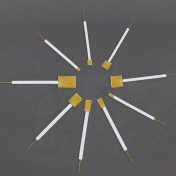
- Gold Electrochemical Sheet Electrode Gold Electrode
- Gold Disc Electrode
People Also Ask
- What is the voltage of e-beam evaporation? Achieve Precise Thin-Film Deposition
- What is the process of e-beam coating? Achieve High-Purity, Precise Thin Films for Your Lab
- What is the container that holds the metal source material called in e-beam evaporation? Ensure Purity and Quality in Your Thin-Film Deposition
- What is the current of e-beam evaporation? A Guide to High-Purity Thin Film Deposition
- What is the temperature of e-beam evaporation? Mastering the Two-Zone Thermal Process for Precision Films