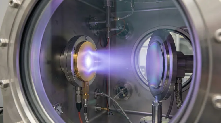
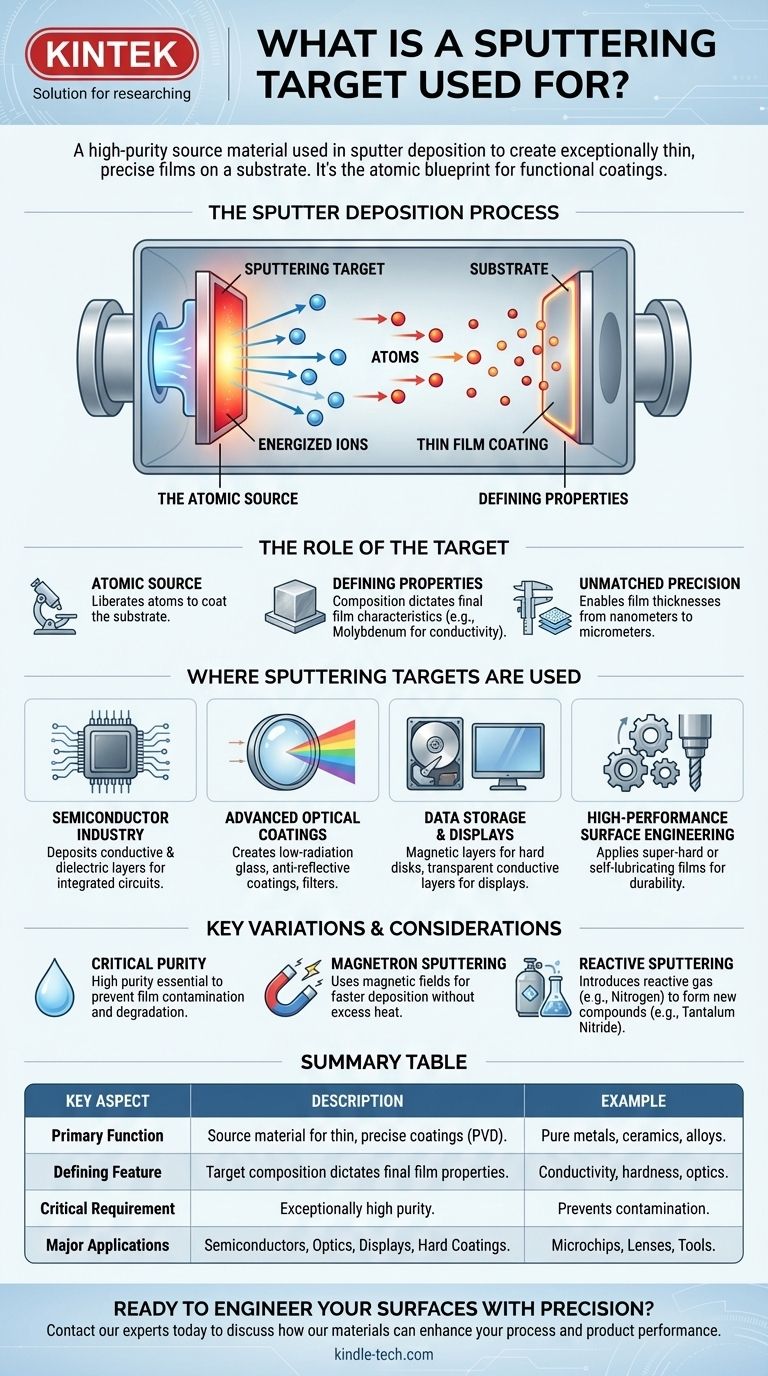
A sputtering target is the high-purity source material used in a process called sputter deposition to create exceptionally thin, precise films on a substrate. This technique involves bombarding the target with energized ions inside a vacuum chamber, which ejects atoms from the target's surface. These ejected atoms then travel and deposit onto another object, forming a highly controlled coating that is fundamental to manufacturing countless modern technologies.
The sputtering target is not merely a piece of material; it is the atomic blueprint for a functional coating. The composition of the target directly dictates the properties of the final thin film, making it the critical starting point for engineering surfaces in everything from microchips to advanced optical lenses.
The Role of the Target in Sputter Deposition
Sputter deposition is a physical vapor deposition (PVD) method, a class of techniques used to build materials layer by layer at the atomic level. The sputtering target is the centerpiece of this entire process.
The Target as the Atomic Source
Think of sputtering as a microscopic, atomic-scale sandblaster. Instead of eroding a surface, the "sand" (energized ions) knocks individual atoms off the target material.
These liberated atoms then coat a nearby object, known as the substrate, building a new, ultra-thin layer. The chemical and physical nature of this new film is a direct copy of the target material.
Defining the Final Film's Properties
The choice of sputtering target is paramount because it defines the characteristics of the final product.
A target made of molybdenum, for instance, is used to create conductive thin films for solar cells and displays. A ceramic target might be used to create an insulating layer in a semiconductor device.
Enabling Unmatched Precision
The primary value of sputtering is its precision. The process allows for the creation of films with thicknesses ranging from just a few nanometers to several micrometers.
This level of control is essential for applications where even the slightest imperfection can cause a component to fail, such as in the intricate layers of a microprocessor.
Where Sputtering Targets Are Used in Practice
The applications for sputter deposition are vast and underpin many high-tech industries. The sputtering target is the starting point for all of them.
In the Semiconductor Industry
Sputtering is a cornerstone of microelectronics manufacturing. It is used to deposit the various conductive and dielectric (insulating) layers required to build integrated circuits, the brains of all modern electronics.
For Advanced Optical Coatings
Sputtering creates films with specialized optical properties. This is used to produce low-radiation glass for energy-efficient windows, anti-reflective coatings for lenses, and filters that transmit or block specific wavelengths of light.
In Data Storage and Displays
The technology was one of the earliest methods used to produce computer hard disks, depositing the magnetic layers that store data. It remains crucial for manufacturing CDs, DVDs, and the transparent conductive layers found in modern flat-panel displays.
For High-Performance Surface Engineering
In the machining industry, sputtering is used to apply super-hard or self-lubricating films to tools and components. This dramatically increases their durability and reduces friction, extending their operational life.
Understanding Key Variations and Considerations
While the basic principle is simple, the sputtering process has several variations and requires careful control to be effective.
The Critical Need for Purity
The sputtering target must be exceptionally pure. Any impurity or contaminant within the target material will be ejected along with the desired atoms and deposited into the final film, potentially degrading its performance.
Magnetron Sputtering
A common enhancement is magnetron sputtering, which uses powerful magnetic fields to trap electrons near the target's surface. This increases the efficiency of the ion bombardment, resulting in faster deposition rates without damaging the substrate with excess heat.
Reactive Sputtering
This advanced technique introduces a reactive gas, like nitrogen or oxygen, into the vacuum chamber along with the standard inert gas. The sputtered atoms from the target react with this gas before reaching the substrate, forming an entirely new compound. For example, sputtering a tantalum target in a nitrogen atmosphere creates tantalum nitride, a material widely used for thin-film resistors.
Making the Right Choice for Your Goal
The selection of a sputtering target and process is driven entirely by the desired outcome for the final thin film.
- If your primary focus is creating conductive pathways: You will use a sputtering target made from a pure metal like molybdenum, copper, or gold, essential for semiconductor and display manufacturing.
- If your primary focus is achieving specific optical properties: The target material must be chosen for its unique refractive index to create coatings for lenses, mirrors, and specialized glass.
- If your primary focus is developing durable, functional surfaces: You may use a ceramic target or employ reactive sputtering to create super-hard or self-lubricating films for industrial components.
Ultimately, the sputtering target is the foundational element for engineering materials at the atomic level, enabling the precision and performance of countless modern technologies.
Summary Table:
| Key Aspect | Description |
|---|---|
| Primary Function | Source material for depositing thin, precise coatings via sputter deposition (a PVD method). |
| Defining Feature | Target composition directly dictates the final film's properties (conductivity, hardness, optics). |
| Common Materials | Pure metals (e.g., Molybdenum, Gold), Ceramics, Alloys. |
| Critical Requirement | Exceptionally high purity to prevent film contamination. |
| Major Applications | Semiconductors, Optical Coatings, Displays, Data Storage, Hard Coatings for Tools. |
Ready to engineer your surfaces with precision? The right sputtering target is the first step to achieving the exact thin-film properties you need for your semiconductors, optical components, or industrial tools. KINTEK specializes in providing high-purity lab equipment and consumables, including sputtering targets, to meet the demanding requirements of modern laboratories and manufacturing. Contact our experts today to discuss how our materials can enhance your process and product performance.
Visual Guide
Related Products
- Reference Electrode Calomel Silver Chloride Mercury Sulfate for Laboratory Use
- Multifunctional Electrolytic Electrochemical Cell Water Bath Single Layer Double Layer
- Molybdenum Tungsten Tantalum Special Shape Evaporation Boat
- Hemispherical Bottom Tungsten Molybdenum Evaporation Boat
- Cylindrical Press Mold with Scale for Lab
People Also Ask
- Why is the selection of a high-quality reference electrode critical in the electrochemical synthesis? | KINTEK
- Which electrode is used as a reference electrode for measuring half-cell potentials? Understanding the Universal Standard
- What is the recommended maintenance for the filling solution of a reference electrode? A Guide to Stable & Accurate Readings
- Which electrode is used as a reference? A Guide to Accurate Electrochemical Measurements
- Which type of electrode can be used as a reference point? Select the Right One for Accurate Measurements


