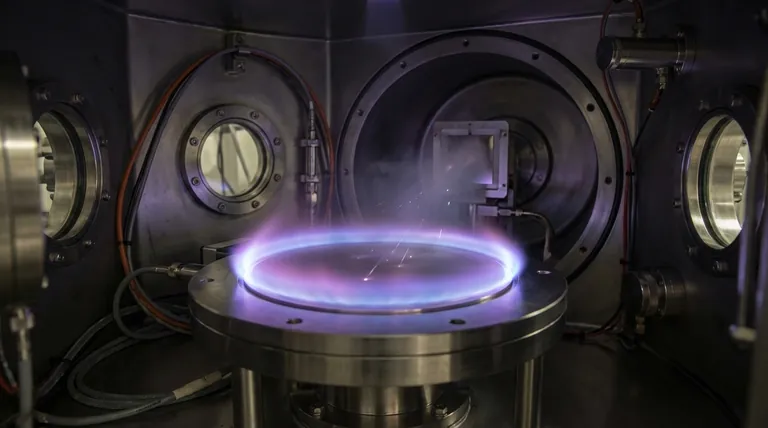
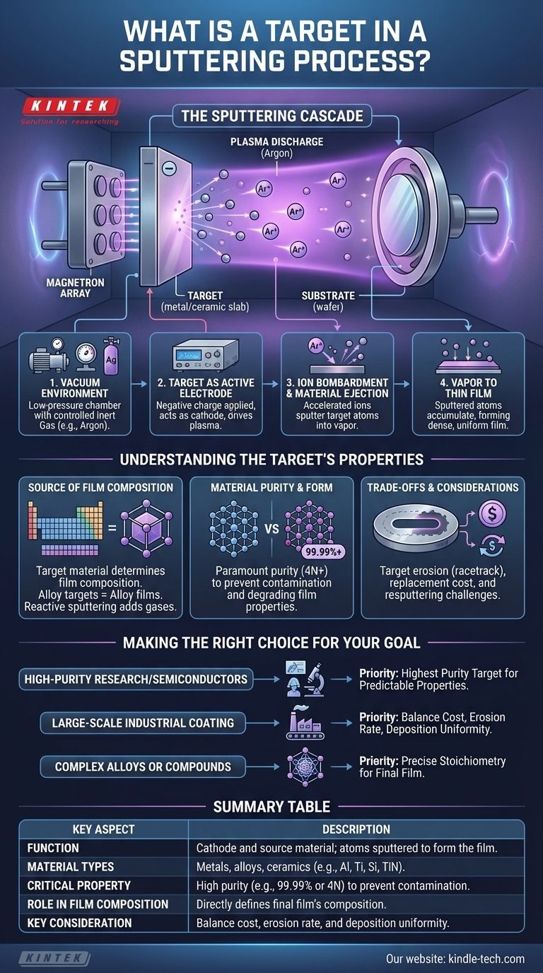
In any sputtering process, the target is the solid source material that is vaporized to create the thin film coating. It is the starting point of the entire deposition process. During sputtering, a slab of the desired coating material—such as a metal, alloy, or ceramic—is placed in a vacuum chamber and bombarded with energetic ions, which physically knock atoms off its surface.
The sputtering target is not merely a passive block of material; it functions as an active cathode and is the definitive source of the final film's chemical composition. The purity, composition, and quality of the target directly dictate the properties and performance of the resulting coating.

The Target's Role in the Sputtering Cascade
To understand the target, you must understand its central role in the sequence of events that define the sputtering process. It is where the thin film originates.
The Vacuum Environment
The entire process occurs inside a high-vacuum chamber, typically backfilled with a small, controlled amount of an inert gas like Argon. This low-pressure environment is critical to prevent contamination and allow the sputtered atoms to travel freely from the target to the substrate.
The Target as an Active Electrode
A high-power, negative DC or RF electrical charge is applied directly to the target, causing it to function as a cathode. This negative potential is the engine that drives the process, creating a glowing plasma discharge in the Argon gas.
Ion Bombardment and Material Ejection
The plasma consists of a mix of electrons and positively charged Argon ions. These positive Argon ions are accelerated by the strong electric field and drawn toward the negatively charged target at high velocity.
Upon impact, the kinetic energy of the Argon ions is transferred to the atoms on the target's surface. If the energy is sufficient, it dislodges or "sputters" atoms from the target material, ejecting them into the vacuum chamber.
From Vapor to Thin Film
These sputtered atoms travel through the chamber and land on the surface of the substrate (such as a silicon wafer, glass panel, or medical implant). As they accumulate, they nucleate and grow into a dense, uniform, and highly adherent thin film. The thickness of this film is precisely controlled by the deposition time and power applied to the target.
Understanding the Target's Properties
The target is the most critical consumable in sputtering. Its characteristics determine what is possible for the final film.
The Source of Your Film's Composition
The simplest rule of sputtering is that the composition of the target determines the composition of the film. If you sputter an aluminum target, you get an aluminum film. If you want a specific alloy, you must use a target made of that same alloy.
This principle is also used in reactive sputtering, where a metallic target (like titanium) is sputtered in the presence of a reactive gas (like nitrogen) to form a compound film (titanium nitride) on the substrate.
Material Purity and Form
Targets are manufactured from a vast range of materials, from pure elements like silicon, titanium, and chromium to complex alloys and ceramic compounds.
The purity of the target is paramount. Any impurities or contaminants present in the target material will be transferred into the growing film, potentially degrading its electrical, optical, or mechanical properties. For this reason, targets are often specified with purities of 99.99% ("4N") or higher.
Key Trade-offs and Considerations
While powerful, the sputtering process and the targets it uses have practical limitations that must be managed.
Target Erosion and Uniformity
The ion bombardment is never perfectly uniform across the target's surface. It tends to concentrate in a "racetrack" pattern, causing the target to erode unevenly. This can affect the uniformity of the coating over time and is why magnetron sputtering systems use moving magnets to help even out this erosion.
Replacement Frequency and Cost
Targets are consumables. While their replacement frequency is relatively low compared to other deposition sources, they eventually wear out and must be replaced. High-purity targets made from precious or exotic materials can represent a significant operational cost, especially in mass production.
The Challenge of "Resputtering"
"Resputtering" occurs when energetic particles in the plasma bombard the substrate itself, knocking off atoms that have already been deposited. This can lower the net deposition rate and alter the final properties of the film. Process parameters must be carefully tuned to minimize this effect.
Making the Right Choice for Your Goal
The choice and management of your target are dictated by your end goal.
- If your primary focus is high-purity research or semiconductors: Your top priority is sourcing the highest-purity target available to ensure your film's properties are predictable and free from contamination.
- If your primary focus is large-scale industrial coating: You must balance target cost with its lifespan (erosion rate) and the deposition rate to optimize throughput and cost-per-part.
- If your primary focus is depositing complex alloys or compounds: Sputtering is ideal, but you must ensure your target has the precise stoichiometry required for the final film, as it will be transferred directly.
Ultimately, understanding that the target is the genesis of your thin film is the first step toward mastering the precise control that sputtering offers.
Summary Table:
| Key Aspect | Description |
|---|---|
| Function | Acts as the cathode and source material; atoms are sputtered off its surface to form the film. |
| Material Types | Metals, alloys, ceramics (e.g., Aluminum, Titanium, Silicon, Titanium Nitride). |
| Critical Property | High purity (e.g., 99.99% or 4N) to prevent film contamination. |
| Role in Film Composition | The target's chemical composition directly defines the final film's composition. |
| Key Consideration | Balance between cost, erosion rate, and deposition uniformity for your application. |
Ready to achieve precise, high-quality thin films? The right sputtering target is critical for your lab's success. At KINTEK, we specialize in providing high-purity lab equipment and consumables, including sputtering targets tailored to your research or production needs. Whether you're in semiconductors, industrial coating, or advanced materials research, our expertise ensures you get the optimal materials for superior film properties and performance. Contact us today to discuss your specific requirements and let KINTEK be your partner in precision coating solutions!
Visual Guide
