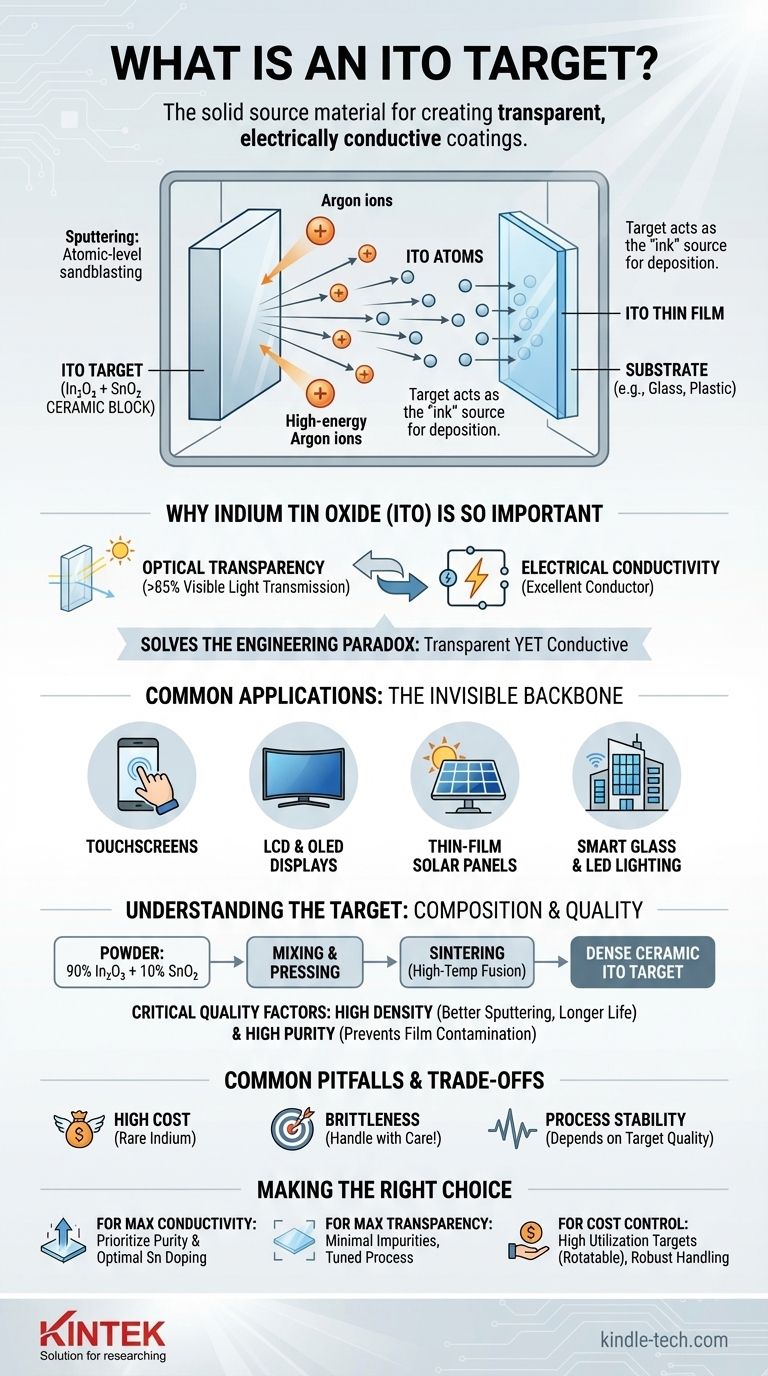
In simple terms, an ITO target is the solid source material used to create transparent, electrically conductive coatings on surfaces like glass or plastic. It is a dense, ceramic block made from a precise mixture of indium oxide (In₂O₃) and tin oxide (SnO₂) powders, which serves as the "ink" in a high-tech deposition process called sputtering.
The ITO target is not the final coating itself, but rather the raw material that is physically vaporized atom-by-atom to form the essential thin films that power devices like touchscreens, solar panels, and flat-panel displays.
The Role of the ITO Target in Sputtering
To understand the target, you must first understand the process it's designed for. The target is a critical component in a widely used manufacturing technique called Physical Vapor Deposition (PVD), specifically magnetron sputtering.
What is Sputtering?
Sputtering is a vacuum deposition method. Think of it as a microscopic, atomic-level sandblaster.
Inside a vacuum chamber, high-energy ions (typically from an inert gas like Argon) are accelerated and directed at the ITO target.
This bombardment has enough force to knock individual atoms or molecules off the surface of the target, launching them into the vacuum.
The Target as the Source Material
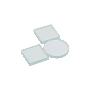
The ITO target acts as the solid source—the material to be deposited. It is typically manufactured into a specific shape, like a flat plate or a rotatable cylinder, to fit into the sputtering equipment.
The material ejected from the target is what will eventually form the final, ultra-thin coating.
From Target to Thin Film
Once knocked loose, the ITO atoms travel through the vacuum chamber and land on a substrate, such as a sheet of glass or flexible film.
They condense on this surface, gradually building up a layer that is uniform and often only a few hundred nanometers thick. This deposited layer is the ITO thin film.
Why Indium Tin Oxide (ITO) is So Important
The reason for this complex process comes down to the unique and valuable properties of ITO itself. It solves a fundamental engineering paradox.
The Unique Combination: Transparency and Conductivity
Most materials that conduct electricity well, like copper or aluminum, are opaque. Most materials that are transparent, like glass, are electrical insulators.
ITO is one of the few materials that excels at both. It is optically transparent (letting over 85% of visible light pass through) while also being an excellent electrical conductor.
Common Applications
This dual property makes ITO indispensable for countless modern technologies. It is the invisible backbone of:
- Touchscreens: Providing the conductive grid that senses your finger's position.
- LCD and OLED Displays: Serving as the transparent top electrode to control the pixels.
- Thin-Film Solar Panels: Acting as a transparent top contact to extract electricity without blocking sunlight.
- Smart Glass and LED Lighting: Enabling transparent conductive pathways.
Understanding the Target's Properties
The quality and composition of the ITO target directly dictate the performance of the final thin film. Manufacturers go to great lengths to control its characteristics.
From Powder to Solid Ceramic
The target begins as high-purity indium oxide and tin oxide powders. A common ratio is 90% In₂O₃ to 10% SnO₂ by weight.
These powders are mixed, pressed, and then sintered—a high-temperature process that fuses the powder into a dense, stable, and solid ceramic block ready for use.
The Importance of Density and Purity
The performance of the sputtering process depends heavily on the target's quality.
A high-density target sputters more evenly and lasts longer. High purity is crucial because even trace contaminants can degrade the electrical conductivity or optical transparency of the final film.
Common Pitfalls and Trade-offs
While ITO is a cornerstone material, working with it involves significant challenges that every engineer and operator must consider.
The High Cost of Indium
Indium is a rare and expensive element. Consequently, ITO sputtering targets represent a significant portion of the manufacturing cost for many electronic devices.
Brittleness and Handling
As a ceramic material, an ITO target is very brittle. It can easily crack or shatter if mishandled, dropped, or subjected to thermal shock (heating or cooling too quickly), leading to costly downtime.
Process Stability
Maintaining a consistent sputtering rate is key to producing uniform films. Variations in target density or impurities can lead to arcing or process instability, resulting in defective products.
Making the Right Choice for Your Goal
Selecting and managing an ITO target is about balancing performance, cost, and process stability based on the final application.
- If your primary focus is maximum conductivity: Prioritize a target with high purity and the optimal tin-doping ratio, as this is critical for charge carrier mobility in the film.
- If your primary focus is optical transparency: Ensure the target material has minimal impurities and that the sputtering process is finely tuned to create a smooth, non-absorptive film.
- If your primary focus is cost control: Focus on targets with high material utilization rates (like rotatable targets) and implement robust handling procedures to prevent breakage.
Ultimately, understanding the ITO target is the first step toward mastering the art of creating high-performance transparent conductive films.
Summary Table:
| Key Aspect | Description |
|---|---|
| Material Composition | Ceramic block of 90% Indium Oxide (In₂O₃) and 10% Tin Oxide (SnO₂) |
| Primary Function | Source material for sputtering to create transparent conductive coatings |
| Key Properties | High electrical conductivity + >85% optical transparency |
| Common Applications | Touchscreens, LCD/OLED displays, solar panels, smart glass |
| Manufacturing Process | Powder mixing, pressing, and high-temperature sintering |
| Critical Quality Factors | High density, high purity, precise composition control |
Ready to optimize your transparent conductive film production?
KINTEK specializes in high-performance lab equipment and consumables for advanced materials research and development. Whether you're developing next-generation displays, solar panels, or touch interfaces, our expertise in sputtering targets and deposition technologies can help you achieve superior film quality and process efficiency.
Contact our experts today to discuss how we can support your specific application needs with reliable solutions and technical guidance.
Visual Guide
Related Products
- Laboratory CVD Boron Doped Diamond Materials
- Reference Electrode Calomel Silver Chloride Mercury Sulfate for Laboratory Use
- Multifunctional Electrolytic Electrochemical Cell Water Bath Single Layer Double Layer
- Battery Lab Equipment 304 Stainless Steel Strip Foil 20um Thick for Battery Test
- Hemispherical Bottom Tungsten Molybdenum Evaporation Boat
People Also Ask
- Are CVD diamonds good? Real Diamonds with Ethical Origins & Better Value
- Are CVD diamonds synthetic? Discover the Truth About Lab-Grown Diamonds
- Do CVD diamonds pass diamond tester? Yes, they are real diamonds.
- What are the advantages of BDD electrodes? Maximize Wastewater Treatment Efficiency and Durability
- What is the purpose of performing anodic polarization on BDD electrodes? Ensure Accurate & Reproducible Research Results