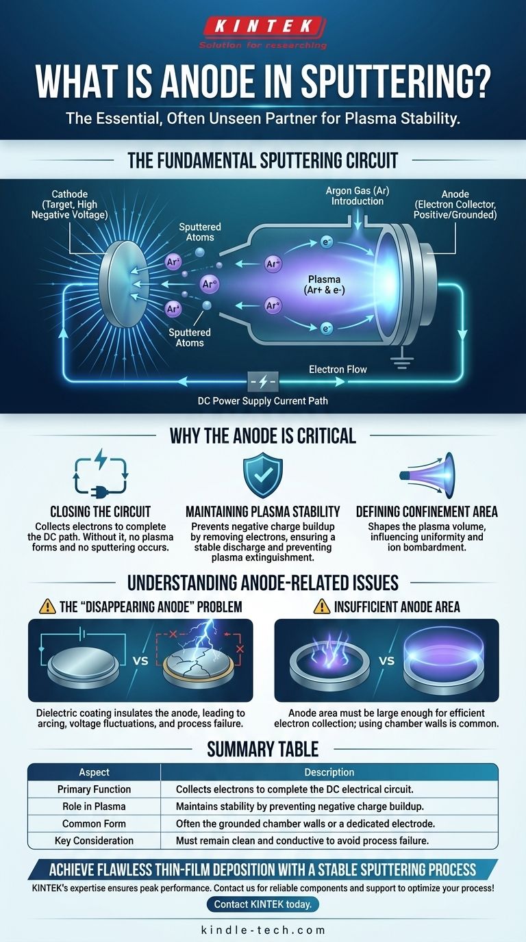
In a sputtering system, the anode is the positively charged electrode responsible for collecting electrons and completing the electrical circuit necessary to sustain the plasma. While the cathode (the target) gets most of the attention, the anode is the essential, often unseen, partner that makes the entire deposition process possible.
The anode's role is not passive. It actively maintains the plasma by completing the DC circuit, ensuring a stable flow of current and preventing charge buildup that would otherwise extinguish the sputtering process.
The Fundamental Circuit of a Sputtering System
To understand the anode, you must first visualize the sputtering system as a simple DC electrical circuit operating in a vacuum. This circuit has two primary components: the cathode and the anode.
The Cathode (The Target)
The cathode is given a high negative voltage. This component is also the target, which is the source material (e.g., titanium, gold, silicon dioxide) you intend to deposit as a thin film.
The Anode (The Electron Collector)
The anode is the corresponding positive or grounded electrode. Its primary function is to attract and collect the free electrons that are generated within the system. In many simple sputtering setups, the grounded vacuum chamber walls and other fixtures serve as the anode.
The Plasma (The Working Medium)
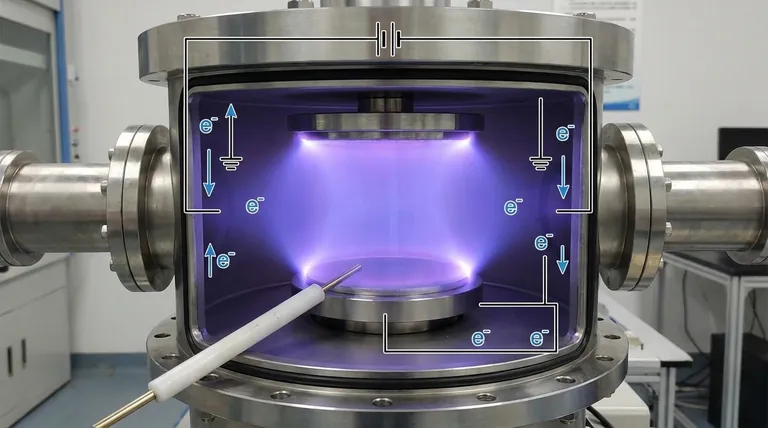
An inert gas, typically argon, is introduced into the chamber. The strong electric field between the cathode and anode energizes this gas, stripping electrons from the argon atoms and creating a glowing discharge known as plasma.
This plasma is a mixture of positive argon ions (Ar+) and free electrons (e-). The positive argon ions are accelerated by the electric field and forcefully collide with the negatively charged cathode (target), knocking off, or "sputtering," atoms of the target material.
Why the Anode is Critical for a Stable Process
The anode’s function goes far beyond simply being the "other end" of the circuit. It is essential for creating a stable and continuous process.
Closing the Electrical Circuit
Without an anode to collect electrons, there is no complete path for current to flow. The power supply would be unable to establish a potential, no plasma could be formed, and no sputtering would occur. The anode provides the return path for the electrical current.
Maintaining Plasma Stability
As the plasma generates a massive number of free electrons, they must be removed from the system. The anode attracts these negatively charged electrons, preventing a negative space charge from building up in the chamber.
If this charge were allowed to accumulate, it would begin to repel the very electrons needed to sustain the plasma, causing the plasma to become unstable or even extinguish itself.
Defining the Plasma Confinement Area
The location and surface area of the anode help define the volume where the plasma is most stable. The electric field lines terminate on the anode, shaping the plasma and influencing the uniformity of the ion bombardment on the target.
Understanding Anode-Related Issues
Because its role can seem passive, the anode is often the source of overlooked process problems.
The "Disappearing Anode" Problem
This is the most common anode-related failure. If you are sputtering a dielectric (insulating) material, a thin, non-conductive layer can accidentally coat the anode surface.
This coating insulates the anode from the plasma. As the conductive surface area "disappears," the power supply struggles to maintain a stable current, leading to arcing, voltage fluctuations, and process failure.
Insufficient Anode Area
For a stable plasma, the surface area of the anode should generally be at least as large as the surface area of the cathode. If the anode is too small, it can't collect electrons efficiently, leading to an unstable discharge. This is why using the entire chamber body as the anode is a common and effective design.
Key Considerations for Your Sputtering Process
- If your primary focus is process stability: Ensure your anode, whether it's the chamber walls or a dedicated electrode, remains clean and free of insulating coatings.
- If your primary focus is system design: For most DC sputtering applications, designing the system so the grounded chamber serves as the anode is the simplest and most reliable configuration.
- If you are troubleshooting an unstable plasma: One of the first things to investigate is the condition of your anode. Check for signs of coating and ensure all electrical connections are secure.
The anode is the quiet, indispensable foundation of the sputtering process, enabling the stable electrical environment required for high-quality thin-film deposition.
Summary Table:
| Aspect | Description |
|---|---|
| Primary Function | Collects electrons to complete the DC electrical circuit. |
| Role in Plasma | Maintains stability by preventing negative charge buildup. |
| Common Form | Often the grounded chamber walls or a dedicated electrode. |
| Key Consideration | Must remain clean and conductive to avoid process failure. |
Achieve flawless thin-film deposition with a stable sputtering process. The anode is a critical component for maintaining plasma stability, and KINTEK's expertise in lab equipment ensures your sputtering system operates at peak performance. Whether you need reliable components, system design consultation, or troubleshooting support for your laboratory, we are here to help. Contact KINTEK today to optimize your deposition process!
Visual Guide
Related Products
- Graphite Vacuum Furnace Negative Material Graphitization Furnace
- Spark Plasma Sintering Furnace SPS Furnace
People Also Ask
- What is the disadvantage of graphite furnace? Managing Reactivity and Contamination Risks
- What is the principle of graphite furnace? Achieve Extreme Temperatures with Direct Resistive Heating
- What are the advantages of graphite furnace? Achieve High-Temperature Precision and Purity
- What is the use of graphite furnace? Achieve Extreme-Temperature Processing for Advanced Materials
- What is the graphite furnace used for? Achieve Extreme Heat Up to 3000°C in a Controlled Environment