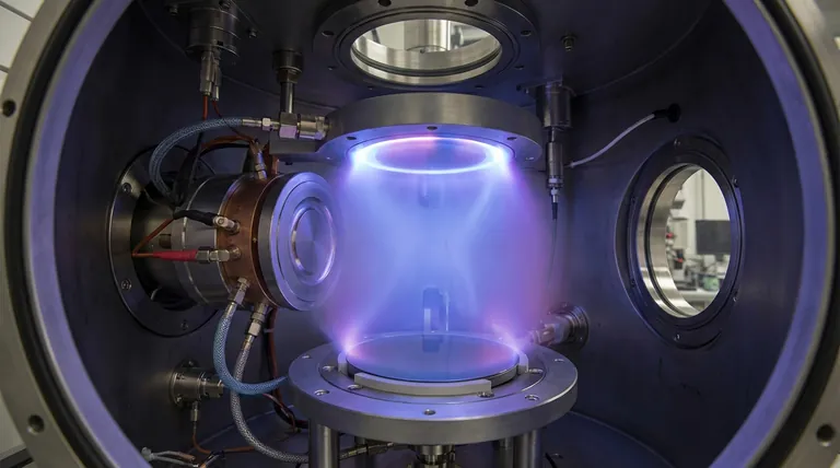
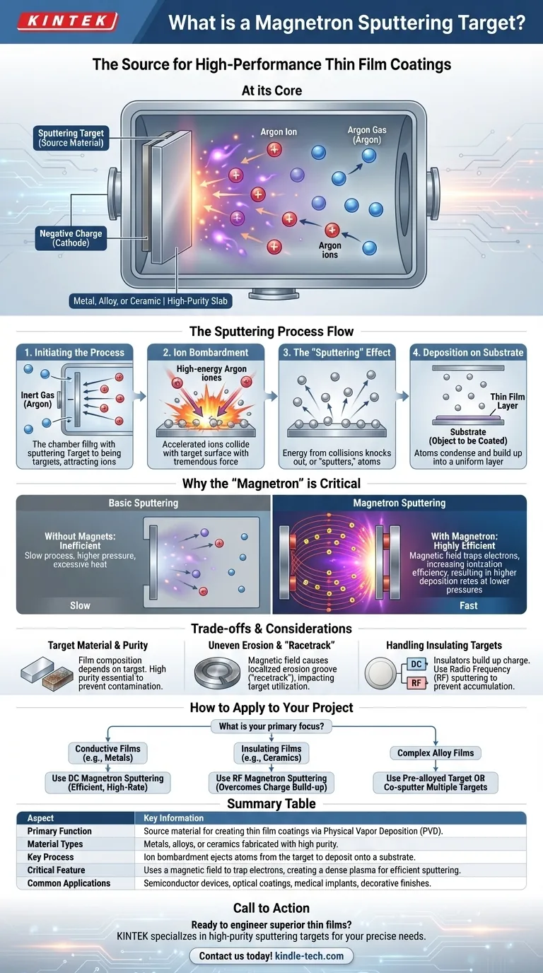
At its core, a magnetron sputtering target is the source material for creating a high-performance thin film coating. It is a precisely fabricated slab of metal, alloy, or ceramic that is methodically vaporized inside a vacuum chamber. Energetic ions bombard the target, knocking atoms loose, which then travel and deposit onto a substrate to form an ultra-thin, uniform layer with specific optical, electrical, or mechanical properties.
The magnetron sputtering target is not just a piece of material; it is the fundamental starting point of a sophisticated deposition process. The key is using a magnetic field to concentrate a plasma, which enables a highly efficient and controlled bombardment of the target to create superior thin films at lower temperatures and pressures than other methods.
The Role of the Target in the Sputtering Process
Magnetron sputtering is a type of Physical Vapor Deposition (PVD), meaning it's a mechanical process, not a chemical one. The target is the central player in this physical transfer of material.
Initiating the Process: The Target as a Cathode
The process begins inside a low-pressure vacuum chamber filled with an inert gas, typically Argon. The sputtering target is given a strong negative electrical charge, making it the cathode.
Generating the Coating Material: Ion Bombardment
This negative charge attracts positively charged Argon ions from the surrounding plasma. These ions accelerate and collide with the target's surface with tremendous force. Think of it as a sandblaster operating at an atomic scale.
The "Sputtering" Effect: Ejecting Atoms
The energy from these collisions is enough to knock out, or "sputter," individual atoms from the target material. These ejected atoms fly off the target in various directions, traveling through the vacuum environment.
Deposition: Forming the Film on a Substrate
These sputtered atoms eventually strike the substrate—the object being coated (such as a silicon wafer, glass pane, or medical implant). Upon arrival, they condense and build up, layer by layer, to form a dense, high-purity thin film.
Why the "Magnetron" is the Critical Component
Simply applying a voltage to sputter a target is inefficient. The "magnetron" part of the name refers to the use of powerful magnets, which dramatically improves the speed and quality of the process.
The Problem with Basic Sputtering
Without a magnetic field, the process is slow, requires higher gas pressures, and can generate excessive heat. The plasma is diffuse and weak, leading to a low rate of ion bombardment.
The Solution: Confining the Plasma
In magnetron sputtering, a set of strong magnets is placed behind the target. This magnetic field traps free electrons from the plasma, forcing them into a spiral path very close to the target's surface.
Increasing Ionization Efficiency
These trapped, spiraling electrons have a much higher probability of colliding with neutral Argon gas atoms. Each collision can knock an electron off an Argon atom, creating another positive Argon ion. This self-sustaining cascade creates a very dense, intense plasma concentrated directly in front of the target.
The Result: Higher Deposition Rates
A denser plasma means far more ions are available to bombard the target. This results in a significantly higher sputtering rate, making the process faster, more energy-efficient, and capable of operating at lower pressures, which improves the quality of the resulting film.
Understanding the Trade-offs and Considerations
While powerful, this technique requires careful engineering and an understanding of its limitations to achieve consistent results.
Target Material and Purity
The composition of the final film is directly determined by the target's composition. Therefore, targets must be fabricated with extremely high purity to prevent contamination in the final coating. They can be made from pure metals, complex alloys, or ceramic compounds.
Uneven Erosion and the "Racetrack"
The magnetic field that enhances the process also causes a major drawback: uneven erosion. The ions are concentrated in a specific area, leading to a visible erosion groove often called a "racetrack." This means only a fraction of the target material is consumed before it must be replaced, impacting cost-efficiency.
Handling Insulating Targets
Sputtering a conductive metal target can be done with a simple Direct Current (DC) power supply. However, if the target is an electrical insulator (like a ceramic), positive charge from the ions will build up on its surface, eventually repelling further bombardment and stopping the process.
To overcome this, Radio Frequency (RF) sputtering is used. The rapidly alternating electrical field prevents charge accumulation, allowing for the deposition of insulating materials, though the equipment is more complex.
How to Apply This to Your Project
Your choice of target and sputtering method depends entirely on the material you need to deposit and its intended function.
- If your primary focus is depositing conductive films (e.g., metals for electronics or decorative coatings): DC magnetron sputtering is the efficient, high-rate industry standard for this task.
- If your primary focus is depositing insulating films (e.g., ceramics for optical filters or protective barriers): RF magnetron sputtering is necessary to overcome charge build-up on the non-conductive target material.
- If your primary focus is creating complex alloy films: You can use a single, pre-alloyed target or co-sputter from multiple elemental targets simultaneously to achieve precise chemical compositions.
Ultimately, understanding the sputtering target is the first step toward mastering the process of engineering materials at the atomic level.
Summary Table:
| Aspect | Key Information |
|---|---|
| Primary Function | Source material for creating thin film coatings via Physical Vapor Deposition (PVD). |
| Material Types | Metals, alloys, or ceramics fabricated with high purity. |
| Key Process | Ion bombardment ejects atoms from the target to deposit onto a substrate. |
| Critical Feature | Uses a magnetic field to trap electrons, creating a dense plasma for efficient sputtering. |
| Common Applications | Semiconductor devices, optical coatings, medical implants, decorative finishes. |
Ready to engineer superior thin films for your project?
The right magnetron sputtering target is fundamental to achieving the specific optical, electrical, or mechanical properties your application demands. KINTEK specializes in high-purity lab equipment and consumables, including sputtering targets, to serve your precise laboratory needs.
Contact us today to discuss how our solutions can enhance your deposition process and bring your material designs to life.
Get in touch with our experts now!
Visual Guide
Related Products
- Boron Nitride (BN) Ceramic Plate
- Molybdenum Tungsten Tantalum Special Shape Evaporation Boat
- Hemispherical Bottom Tungsten Molybdenum Evaporation Boat
- Reference Electrode Calomel Silver Chloride Mercury Sulfate for Laboratory Use
- Microwave Plasma Chemical Vapor Deposition MPCVD Machine System Reactor for Lab and Diamond Growth
People Also Ask
- What type of brazing works at lower temperature? Silver Alloys for Heat-Sensitive Materials
- What is the easiest to melt metal? Start with Tin and Pewter for Safe, Simple Casting
- What is the necessity of using a ceramic crucible as a carrier during BN synthesis? Ensure High-Purity Results
- What are the target materials for sputtering? From Metals to Ceramics for Precise Thin Films
- What is sputtering target material? The Blueprint for High-Quality Thin Film Coatings