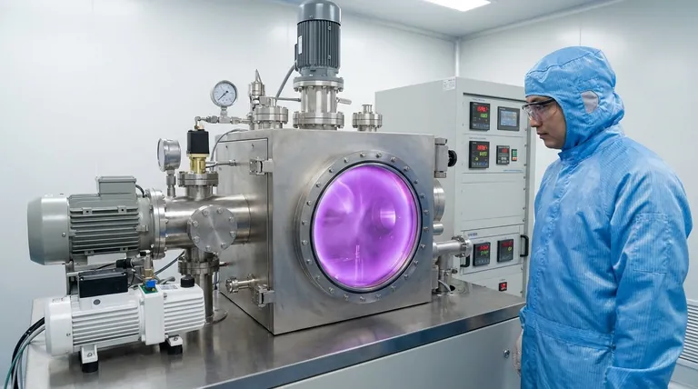
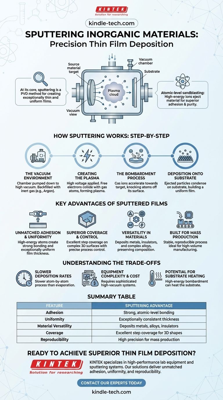
At its core, sputtering is a physical vapor deposition (PVD) method used to create exceptionally thin and uniform films of inorganic materials. The process uses high-energy ions to bombard a source material inside a vacuum, physically knocking atoms or molecules off its surface. These ejected particles then travel and deposit onto a target object, known as a substrate, forming the desired coating.
Sputtering is less like spraying a coating and more like atomic-level sandblasting. It uses energized gas ions to methodically eject material from a source target, ensuring the resulting film has superior adhesion, purity, and uniformity compared to other methods.
How Sputtering Works: A Step-by-Step Breakdown
The sputtering process is a highly controlled sequence that takes place within a specialized vacuum chamber. Each step is critical to achieving a high-quality film.
The Vacuum Environment
First, the substrate and the source material (the target) are placed inside a sealed chamber. The chamber is pumped down to a high vacuum to remove air and other contaminants. It is then backfilled with a small, controlled amount of an inert gas, such as Argon.
Creating the Plasma
A high voltage is applied, causing the source material target to become negatively charged (a cathode). This electrical field accelerates free electrons, which collide with the neutral inert gas atoms. These collisions strip electrons from the gas atoms, creating a cloud of positively charged ions and free electrons known as a plasma.
The Bombardment Process
The positively charged gas ions are forcefully accelerated toward the negatively charged target. They strike the target's surface with significant kinetic energy. This impact is energetic enough to overcome the atomic bonding forces of the target material, knocking individual atoms or molecules free from the surface.
Deposition onto the Substrate
These ejected particles travel in a straight line through the low-pressure environment until they strike the substrate. Upon arrival, they condense and bond to the substrate's surface, gradually building up a thin, dense, and highly uniform film.
Key Advantages of Sputtered Films
Sputtering is chosen over other deposition techniques for its distinct and powerful advantages, particularly in high-performance applications.
Unmatched Adhesion and Uniformity
Because the sputtered atoms arrive at the substrate with high energy, they embed slightly into the surface, creating strong adhesion. The process also ensures an exceptionally uniform film thickness across the entire substrate.
Superior Coverage and Control
Sputtering provides excellent step coverage, meaning it can uniformly coat complex, three-dimensional surfaces with sharp edges or trenches. The film thickness is precisely controlled by adjusting the process time and power, allowing for high reproducibility.
Versatility in Materials
Unlike some other methods, sputtering is not limited by a material's melting point. It can be used to deposit a vast range of materials, including pure metals, insulators, and complex alloys, while preserving their original composition.
Built for Mass Production
The stability, control, and high reproducibility of the sputtering process make it ideal for mass production. Its compatibility with single-wafer processing and infrequent target replacement ensures consistent output in high-volume manufacturing environments.
Understanding the Trade-offs
While powerful, sputtering is not a universal solution. Understanding its limitations is key to making an informed decision.
Slower Deposition Rates
Compared to thermal evaporation, sputtering is generally a slower process. The atom-by-atom ejection mechanism, while precise, can take longer to build up a film of a desired thickness.
Equipment Complexity and Cost
Sputtering systems require sophisticated high-vacuum chambers, power supplies, and control systems. This makes the initial equipment investment and ongoing maintenance more costly than simpler deposition methods.
Potential for Substrate Heating
The constant bombardment of high-energy particles can transfer a significant amount of heat to the substrate. For heat-sensitive substrates, this can be a critical issue that requires active cooling or process modification to manage.
Making the Right Choice for Your Application
Selecting a deposition method depends entirely on your project's end goal. Sputtering's value is in its precision and quality.
- If your primary focus is film quality and precision: Sputtering is the definitive choice for applications demanding superior adhesion, density, and uniformity.
- If your primary focus is complex materials: Sputtering excels at depositing alloys and compounds with high compositional accuracy and reproducibility.
- If your primary focus is high-volume manufacturing: The process's stability and control make it ideal for industrial-scale production where consistency is non-negotiable.
- If your primary focus is speed and low cost for simple films: You may consider alternative methods like thermal evaporation, but you will sacrifice the quality and performance benefits inherent to sputtering.
By understanding its principles, you can leverage sputtering to achieve a level of material deposition quality that is simply unattainable with other methods.
Summary Table:
| Feature | Sputtering Advantage |
|---|---|
| Adhesion | Strong, atomic-level bonding to substrate |
| Uniformity | Exceptionally consistent film thickness |
| Material Versatility | Deposits metals, alloys, and insulators |
| Coverage | Excellent step coverage for complex 3D shapes |
| Reproducibility | High precision and control for mass production |
Ready to achieve superior thin film deposition for your laboratory?
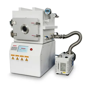
At KINTEK, we specialize in high-performance lab equipment, including sputtering systems designed for precision and reliability. Whether you're working with metals, alloys, or complex inorganic materials, our solutions deliver the unmatched adhesion, uniformity, and reproducibility your research or production demands.
Contact our experts today to discuss how KINTEK's sputtering technology can enhance your lab's capabilities and drive your projects forward.
Visual Guide
Related Products
- Three-dimensional electromagnetic sieving instrument
- Chemical Vapor Deposition CVD Equipment System Chamber Slide PECVD Tube Furnace with Liquid Gasifier PECVD Machine
- Customer Made Versatile CVD Tube Furnace Chemical Vapor Deposition Chamber System Equipment
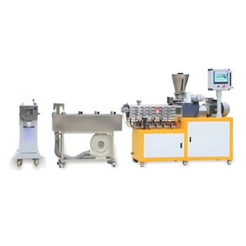
- Twin Screw Extruder Plastic Granulation Machine
- HFCVD Machine System Equipment for Drawing Die Nano-Diamond Coating
People Also Ask
- What are the precautions for sieving method? Ensure Accurate Particle Size Analysis
- Why is sieving equipment necessary for processing powder prior to hot extrusion of PEO? Ensure Cathode Film Uniformity
- What is sieving and how does it work? A Guide to Accurate Particle Size Analysis
- Why is sieving equipment essential for the classification of processed bio-activated carbon? Optimize Performance
- What mixtures can be separated by sieving? A Guide to Efficient Solid-Solid Separation