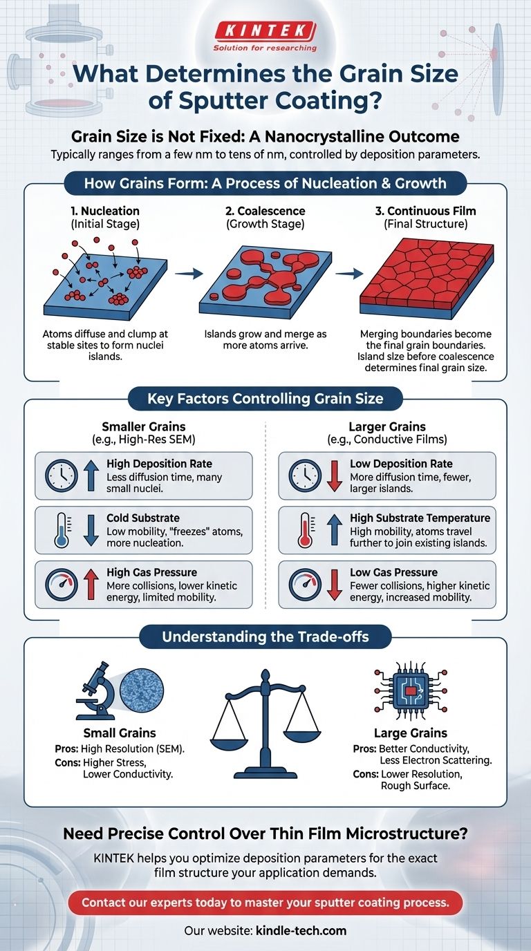
The grain size of a sputter-coated film is not a single fixed value. It is an outcome of the deposition process, typically resulting in an extremely fine, nanocrystalline structure. The final grain size commonly ranges from a few nanometers to several tens of nanometers, depending entirely on the material and the specific process conditions used.
Sputter coating is fundamentally a process of controlled nucleation and growth. The final grain size is not an inherent property of the sputtered material itself, but rather a direct result of manipulating deposition parameters like rate, temperature, and pressure to achieve a desired film structure.

How Grains Form in Sputtered Films
To understand what controls grain size, you must first understand how a sputtered film is built, atom by atom. The process occurs in distinct stages that directly determine the final microscopic structure.
The Initial Stage: Nucleation
Sputtered atoms ejected from the target material do not simply form a uniform layer upon arrival at the substrate. They land with kinetic energy, move across the surface (a process called surface diffusion), and eventually clump together at stable, low-energy sites to form tiny islands, or nuclei.
The Growth Stage: Island Coalescence
These initial nuclei act as seeds. As more atoms arrive, they are more likely to join an existing island than to start a new one. The islands grow larger until they begin to touch and merge, a process known as coalescence.
The Final Structure: Continuous Film
The boundaries where these growing and merging islands finally meet become the grain boundaries in the final, continuous film. The size of the islands just before they fully coalesce is the primary determinant of the film's average grain size.
Key Factors Controlling Grain Size
Because grain size is a result of this growth process, you can control it by tuning the parameters of your sputtering system.
Deposition Rate
The speed at which atoms arrive at the substrate is critical. A high deposition rate gives atoms less time to move around, leading to the formation of many small nuclei. This results in a smaller final grain size. Conversely, a lower rate allows more time for surface diffusion, promoting the growth of fewer, larger islands and thus a larger grain size.
Substrate Temperature
Temperature governs the energy available to the deposited atoms. A higher substrate temperature increases surface mobility, allowing atoms to travel further to join existing islands. This encourages the growth of larger grains. A cold substrate effectively "freezes" atoms where they land, leading to more nucleation sites and a much finer grain structure.
Gas Pressure
Sputtering occurs in a vacuum, but a low-pressure process gas (like Argon) is required to create the plasma. Higher gas pressure increases the chance of sputtered atoms colliding with gas atoms on their way to the substrate. This reduces their kinetic energy upon arrival, limits their surface mobility, and results in smaller grains.
Target Material and Substrate
The inherent properties of the sputtered material (e.g., gold, chromium, platinum) and the substrate surface also play a role. The strength of the bond between the deposited atoms and the substrate influences how easily nuclei can form and grow.
Understanding the Trade-offs
The ideal grain size depends entirely on the application, and optimizing for one property often means compromising on another.
Small Grains: High Resolution vs. High Stress
Extremely fine-grained films, often achieved with noble metals like gold-palladium, are ideal for high-resolution Scanning Electron Microscopy (SEM). The small grains provide a continuous, conductive coating that faithfully replicates the sample's finest features without introducing artifacts. However, these films can have higher internal stress and more grain boundaries, which can impede electrical conductivity.
Large Grains: Better Conductivity vs. Lower Resolution
For applications like creating electrodes or other conductive thin films, larger grains are often desirable. Fewer grain boundaries mean less electron scattering and therefore lower electrical resistivity. The trade-off is that a larger grain structure creates a rougher surface that is unsuitable for high-magnification imaging.
Optimizing Grain Size for Your Application
Choosing the right parameters is about matching the film's physical properties to your ultimate goal.
- If your primary focus is high-resolution SEM imaging: Aim for the smallest possible grains by using a low-energy coater, a suitable gold-palladium or platinum target, and potentially a cooled substrate stage.
- If your primary focus is creating a conductive thin film: Encourage larger grain growth by using a lower deposition rate or slightly elevated substrate temperature to reduce grain boundary density.
- If your primary focus is optical coatings: Balance is critical. You need a smooth, amorphous-like, or very fine-grained film to minimize light scattering, which requires precise control over deposition rate and pressure.
Ultimately, controlling grain size in sputter coating is a matter of precisely tuning your process parameters to build the exact film structure your application demands.
Summary Table:
| Factor | Effect on Grain Size | Typical Goal |
|---|---|---|
| High Deposition Rate | Smaller Grains | High-Resolution SEM Imaging |
| High Substrate Temperature | Larger Grains | Conductive Thin Films |
| High Gas Pressure | Smaller Grains | Smooth Optical Coatings |
| Low Temperature / Rate | Smaller Grains | Fine, Dense Films |
Need precise control over your thin film's microstructure?
The grain size of your sputter-coated film directly impacts its performance, whether for flawless SEM imaging, optimal electrical conductivity, or superior optical properties. At KINTEK, we specialize in lab equipment and consumables that deliver the exact film structure your application demands.
Our expertise helps you optimize deposition parameters to achieve the desired nanocrystalline structure, ensuring your research or production yields consistent, high-quality results.
Contact our experts today to discuss how we can help you master your sputter coating process.
Visual Guide
