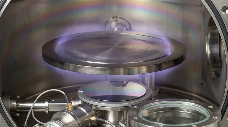
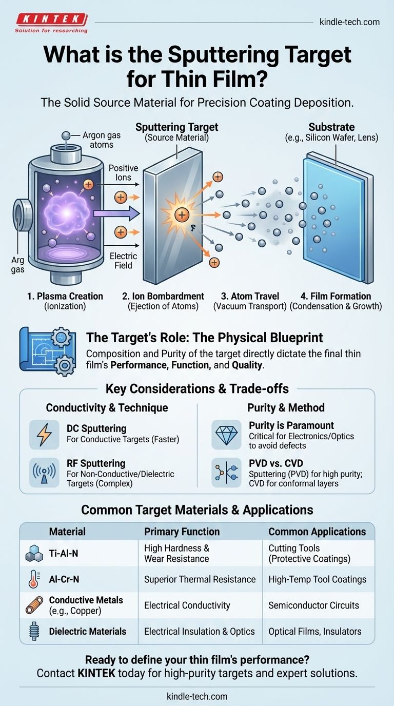
In thin film deposition, the sputtering target is the source material. It is a solid block or plate of the exact substance you wish to deposit as a coating. During the sputtering process, high-energy particles bombard this target, physically knocking atoms off its surface. These ejected atoms then travel and condense onto a substrate, such as a silicon wafer or optical lens, forming an ultra-thin, highly uniform film.
The sputtering target is not just a component; it is the physical blueprint for the final thin film. The composition and purity of the target directly dictate the performance, function, and quality of the finished product, from semiconductor circuits to protective tool coatings.
How Sputtering Works: The Role of the Target
The Basic Principle: Physical Vapor Deposition (PVD)
Sputtering is a Physical Vapor Deposition (PVD) method. This distinguishes it from chemical processes like Chemical Vapor Deposition (CVD).
In PVD, the coating material is physically transformed into a vapor state and then condensed onto the substrate, without underlying chemical reactions defining the process.
The Bombardment Process
The process takes place in a vacuum chamber. An inert gas, typically argon, is introduced and ionized to create a plasma.
An electric field accelerates these positive ions, causing them to collide with the negatively charged sputtering target with great force.
This high-energy impact has a kinetic effect, ejecting or "sputtering" atoms from the target material, similar to how a cue ball breaks a rack of billiard balls.
From Target to Substrate
The dislodged atoms from the target travel through the low-pressure chamber and land on the substrate.
They gradually build up, atom by atom, to form a precisely controlled thin film. This method allows for exceptional control over the film's thickness and uniformity.
Types of Sputtering Targets and Their Purpose
Defining the Film's Properties
The material chosen for the target is entirely dependent on the desired properties of the final coating. The target's composition is directly replicated in the film.
For example, a Titanium-Aluminum-Nitride (Ti-Al-N) target is used to create a film that provides high hardness and wear resistance for cutting tools.
An Aluminum-Chromium-Nitride (Al-Cr-N) target produces a coating with superior thermal resistance, extending tool life in high-temperature applications.
Targets for Different Applications
The function of the final product determines the target material. Sputtering is used to create two main categories of thin films.
Optical thin films are used for anti-reflective coatings on lenses or reflective layers in mirrors. Electrical thin films are essential for manufacturing insulators, conductors, and complex integrated circuits in the semiconductor industry.
Understanding the Trade-offs and Considerations
Conductive vs. Non-Conductive Targets
A key consideration is the electrical conductivity of the target material. This determines which type of sputtering technology can be used.
Direct Current (DC) sputtering is a simpler, faster method, but it generally requires the target material to be electrically conductive.
Radio Frequency (RF) sputtering can be used with non-conductive (insulating or dielectric) targets. This technique expands the range of possible materials for thin film deposition, but is often a more complex process.
Purity is Paramount
The purity of the sputtering target is critical, especially in semiconductor and optical applications.
Any impurities or contaminants present in the target will be transferred to the thin film, potentially degrading or destroying its electrical or optical performance.
Sputtering vs. Other Methods
Sputtering is just one of several deposition techniques. It is prized for its ability to produce very high-purity coatings and its versatility with alloys.
However, in the semiconductor industry, it competes with Chemical Vapor Deposition (CVD), which is often chosen for its ability to create highly precise and conformal layers. The choice between PVD and CVD depends on the specific material, application, and desired film characteristics.
Making the Right Choice for Your Application
The selection of a sputtering target is a foundational decision in any thin film deposition process. Your end goal dictates the material and technique.
- If your primary focus is creating a hard, protective coating: Consider targets made of ceramic compounds like Titanium-Aluminum-Nitride (Ti-Al-N) or Aluminum-Chromium-Nitride (Al-Cr-N) for their excellent wear and thermal resistance.
- If your primary focus is depositing an insulating material: You must use a non-conductive target and employ the RF sputtering technique to successfully deposit the film.
- If your primary focus is manufacturing high-purity electronics: The purity of your target is the single most critical factor, as any contaminants will degrade the final device's electrical properties.
Ultimately, the sputtering target is the fundamental building block that defines the character and performance of your final thin film.
Summary Table:
| Target Material | Primary Function | Common Applications |
|---|---|---|
| Titanium-Aluminum-Nitride (Ti-Al-N) | High hardness, wear resistance | Protective coatings for cutting tools |
| Aluminum-Chromium-Nitride (Al-Cr-N) | Superior thermal resistance | High-temperature tool coatings |
| Conductive Metals (e.g., Copper) | Electrical conductivity | Semiconductor circuits, conductors |
| Non-Conductive/Dielectric Materials | Electrical insulation | Semiconductor insulators, optical films |
Ready to define your thin film's performance? The right sputtering target is critical for achieving the desired hardness, thermal resistance, or electrical properties in your coating. KINTEK specializes in high-purity lab equipment and consumables, including sputtering targets for research and production. Our experts can help you select the ideal material for your specific application, ensuring superior film quality and performance. Contact KINTEK today to discuss your thin film deposition needs!
Visual Guide
Related Products
- Reference Electrode Calomel Silver Chloride Mercury Sulfate for Laboratory Use
- Multifunctional Electrolytic Electrochemical Cell Water Bath Single Layer Double Layer
- Molybdenum Tungsten Tantalum Special Shape Evaporation Boat
- Hemispherical Bottom Tungsten Molybdenum Evaporation Boat
- Cylindrical Press Mold with Scale for Lab
People Also Ask
- Why is the selection of a high-quality reference electrode critical in the electrochemical synthesis? | KINTEK
- What is the recommended maintenance for the filling solution of a reference electrode? A Guide to Stable & Accurate Readings
- What is the reference electrode in potentiometry? The Key to Stable & Accurate Measurements
- Which electrode is used as a reference? A Guide to Accurate Electrochemical Measurements
- Which electrode is used as a reference electrode for measuring half-cell potentials? Understanding the Universal Standard


