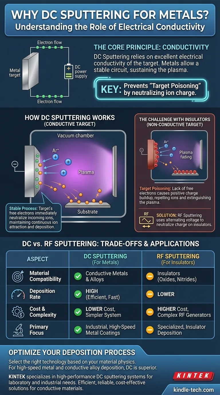
In sputtering, the choice of power supply is dictated by the electrical conductivity of the target material. DC (Direct Current) sputtering is used for metals because they are excellent electrical conductors. This conductivity allows a stable electrical circuit to be completed through the target, which is essential for sustaining the plasma required to eject atoms and deposit them as a thin film. Insulating materials block this current, making the DC method ineffective.
The fundamental reason DC sputtering works for metals is their ability to conduct electricity. This prevents a phenomenon known as "target poisoning," where positive charge builds up on an insulating target surface, repelling the very ions needed to sustain the sputtering process.
How DC Sputtering Works: A Matter of Conductivity
The Basic Sputtering Setup
Sputtering occurs in a vacuum chamber filled with an inert gas, typically argon. Inside are the material to be deposited (the target) and the object to be coated (the substrate). A high DC voltage is applied between them.
Creating the Plasma
This high voltage ionizes the argon gas, stripping electrons from the argon atoms and creating a plasma—a glowing cloud of positive argon ions and free electrons. The target is given a negative charge (making it a cathode) to attract these positive ions.
The Bombardment Process
The positively charged argon ions accelerate towards the negatively charged target, striking it with significant force. This energetic bombardment is strong enough to knock atoms loose from the target material's surface.
Why Metal's Conductivity is Crucial
When the positive argon ions strike the conductive metal target, the target's abundant free electrons immediately neutralize their charge. This allows the target to maintain its strong negative potential, continuously attracting more ions and keeping the sputtering process stable and efficient. The metal target effectively completes the electrical circuit.
The Challenge with Insulating Materials
The Problem of Charge Buildup
If you tried to use DC sputtering with an insulating material like a ceramic or oxide, a critical problem would arise. These materials lack the free electrons needed to neutralize the incoming positive argon ions.
Target "Poisoning" and Plasma Collapse
As positive charge accumulates on the insulator's surface, it creates a localized positive field. This field repels the incoming positive argon ions, stopping the bombardment and effectively extinguishing the plasma. This phenomenon is often called **"target poisoning."
The RF Sputtering Solution
This is why insulating materials require Radio Frequency (RF) sputtering. RF power rapidly alternates the target's voltage from negative to positive. The negative cycle attracts ions for sputtering, while the brief positive cycle attracts electrons from the plasma to neutralize the charge buildup, allowing the process to continue.
Understanding the Trade-offs
Advantage of DC: Deposition Rate
For conductive materials, DC sputtering typically achieves a much higher deposition rate than RF sputtering. This makes it far more efficient for industrial and manufacturing applications where speed is critical.
Advantage of DC: System Simplicity and Cost
DC power supplies are simpler, more robust, and less expensive than the complex RF generators and impedance-matching networks required for RF sputtering. This lowers both the initial investment and a system's operational cost.
Limitation of DC: Material Constraint
The primary and most significant limitation of DC sputtering is its restriction to electrically conductive materials. It is simply not a viable process for depositing pure insulators like oxides and nitrides.
How to Apply This to Your Project
Ultimately, the physics of your target material dictates the correct choice of technology.
- If your primary focus is depositing a pure metal or conductive alloy at high speed: DC sputtering is almost always the superior choice due to its higher deposition rate and equipment simplicity.
- If your primary focus is depositing an insulator like an oxide or nitride: You must use RF sputtering to overcome the issue of target charge buildup.
- If your primary focus is cost-efficiency and high throughput for metal coatings: DC sputtering is the more cost-effective and faster method.
Understanding the electrical properties of your target material is the key to selecting a successful and efficient deposition strategy.
Summary Table:
| Aspect | DC Sputtering (for Metals) | RF Sputtering (for Insulators) |
|---|---|---|
| Material Compatibility | Conductive metals & alloys | Insulators (e.g., oxides, nitrides) |
| Deposition Rate | High | Lower |
| Cost & Complexity | Lower cost, simpler equipment | Higher cost, complex RF generators |
| Key Challenge | N/A (stable for conductors) | Prevents charge buildup on insulators |
Ready to optimize your metal deposition process?
At KINTEK, we specialize in providing high-performance DC sputtering systems tailored for laboratory and industrial applications. Our equipment ensures efficient, reliable thin-film deposition for conductive metals and alloys, helping you achieve faster results with lower operational costs.
Whether you're working on research, prototyping, or production, KINTEK's lab equipment solutions are designed to meet your specific needs.
Contact us today to discuss how our DC sputtering systems can enhance your project's efficiency and success!
Visual Guide