Overview of Sputtering Targets in IC Manufacturing
Technical Requirements for Sputtering Targets
Sputtering targets used in the integrated circuit manufacturing process demand stringent technical requirements to ensure optimal performance and reliability. These targets must exhibit high metal purity, with stringent control over impurity content and defect levels. The purity of these targets typically ranges from 99.9% to 99.9999% (3N to 6N), ensuring that the resulting films are free from contaminants that could degrade device performance.
In addition to purity, grain uniformity and grain direction are critical. The uniformity of grain size and orientation across the target surface ensures consistent film deposition, which is essential for the precise fabrication of integrated circuits. Any variation in grain structure can lead to non-uniform film properties, potentially causing defects in the final product.
Processing accuracy is another key requirement. The targets must be manufactured with high precision to meet the dimensional and structural demands of advanced sputtering equipment. This includes maintaining tight tolerances on parameters such as surface roughness, density, and composition uniformity. For instance, targets used in magnetron sputtering require ultra-fine grains and ultra-high density to achieve efficient and uniform coating.
Furthermore, the material composition and tissue uniformity must be meticulously controlled. This ensures that the deposited films exhibit the desired mechanical, electrical, and magnetic properties. For example, the oxide content and size must be precisely managed to prevent any adverse effects on film adhesion and integrity.
Lastly, the magnetic permeability of certain targets, especially those used in advanced sputtering techniques like HIPIMS (High Power Impulse Magnetron Sputtering), plays a crucial role in the efficiency and quality of the coating process. High magnetic permeability targets facilitate better electron confinement and ion acceleration, leading to denser and more adherent films.

In summary, the technical requirements for sputtering targets in integrated circuit manufacturing are multifaceted, encompassing purity, grain uniformity, processing accuracy, composition control, and magnetic properties. These stringent demands ensure that the targets can deliver high-quality films essential for the reliable and high-performance fabrication of integrated circuits.
High Purity Sputtering Targets
High purity sputtering targets, with purities ranging from 99.9% to 99.9999% (3N to 6N), are critical components in the physical vapor deposition (PVD) process used in the manufacturing of electronic components. These targets are typically made from metals or non-metals and are essential for ensuring the quality and performance of the final products.
KINTEK, a leading manufacturer, specializes in producing high-density, ultra-high purity sputtering targets using advanced technologies such as vacuum melt/casting and hot isostatic pressing (HIP). These targets are available in various configurations, including monoblock or bonded forms, with dimensions up to 820 mm. They are meticulously designed with features like hole drill locations, threading, beveling, grooves, and backing to ensure compatibility with both standard guns and the latest processing equipment for DC, FM, RF, and HIPIMS/HPPMS sputtering techniques.
In addition to standard sizes, KINTEK also offers research-sized targets and custom options to meet specific requirements. All targets and evaporation materials undergo rigorous analysis using state-of-the-art techniques such as X-Ray Fluorescence (XRF), Glow Discharge Mass Spectrometry (GDMS), and Inductively Coupled Plasma (ICP) to ensure their high purity and quality.
Furthermore, KINTEK provides bulk evaporation materials in various forms, including pellets, rods, pieces, granules, slugs, lumps, ingots, shot, and deposition cones, catering to a wide range of applications in the semiconductor industry.
Specific Applications of Sputtering Targets
Aluminum (Al) and Its Alloy Targets
High-purity aluminum (Al) and its alloy targets play a crucial role in the back-end metal interconnect process of integrated circuits, particularly in the 0.13µm technology node. These targets are essential for achieving the fine linewidths and high conductivity required in modern semiconductor devices. The purity of these aluminum targets typically ranges from 99.9% to 99.9999% (3N to 6N), ensuring minimal impurities that could affect the performance and reliability of the interconnects.
In the context of integrated circuit manufacturing, aluminum and its alloys are primarily used for creating metal layers that connect different components within the chip. The 0.13µm technology node represents a critical milestone where the industry transitioned to more advanced and miniaturized designs, necessitating materials with superior electrical and mechanical properties. The use of high-purity aluminum targets in this process ensures that the resulting metal films exhibit excellent uniformity and low defect rates, which are vital for maintaining signal integrity and reducing resistance.
The alloying of aluminum with elements such as copper (Cu) and silicon (Si) further enhances its performance in specific applications. For instance, aluminum-copper alloys are known for their improved electromigration resistance, which is crucial in high-current density environments. Additionally, the inclusion of silicon in aluminum alloys helps in reducing the formation of hillocks and whiskers, which can cause short circuits in the interconnects.
Moreover, the precise control of grain size and orientation in these high-purity aluminum targets is essential for achieving the desired mechanical and electrical properties. This control is achieved through advanced manufacturing techniques that ensure the targets meet the stringent requirements of the semiconductor industry. The uniformity of these properties across the target surface is critical for the consistency of the deposited film, which directly impacts the yield and performance of the final integrated circuit.
In summary, high-purity aluminum and its alloy targets are indispensable in the 0.13µm technology node and beyond, enabling the fabrication of high-performance and reliable metal interconnects in integrated circuits. Their superior purity, combined with optimized alloy compositions and precise manufacturing processes, ensures that these targets meet the demanding standards of the semiconductor industry.
Titanium (Ti) Targets
High purity titanium (Ti) targets play a crucial role in the physical vapor deposition (PVD) process, particularly in the fabrication of high purity titanium metal films. These targets are predominantly utilized in technology nodes ranging from 0.13µm and above, where the stringent purity requirements are essential for maintaining the integrity and performance of the integrated circuits.
The primary function of these titanium targets is to facilitate the deposition of uniform and high-quality titanium films, which are integral to the functionality and reliability of semiconductor devices. The high purity of these targets, typically ranging from 99.9% to 99.9999% (3N to 6N), ensures that the resulting films are free from impurities that could compromise the device's performance.
In addition to their use in the 0.13µm technology node, titanium targets are also employed in more advanced nodes, where their ability to produce consistent and defect-free films is paramount. This underscores the versatility and robustness of titanium targets in meeting the evolving demands of semiconductor manufacturing.
Furthermore, the high processing accuracy and uniformity of grain direction in these targets contribute to the overall efficiency and effectiveness of the PVD process. This ensures that the titanium films adhere well to the substrate and exhibit the desired mechanical and electrical properties, thereby enhancing the overall performance of the integrated circuits.
Copper (Cu) and Its Alloy Targets
Copper has emerged as a preferred metal interconnect material, gradually replacing aluminum starting from the 0.13µm technology node. This transition is driven by the need for high-purity copper metal targets, which are essential for maintaining the integrity and performance of integrated circuits. The shift to copper interconnects is primarily due to copper's superior electrical conductivity and lower resistance compared to aluminum, which is crucial for reducing signal delays and power consumption in advanced semiconductor devices.
High-purity copper targets, typically with a purity of 99.9% to 99.9999% (3N to 6N), are meticulously crafted to meet the stringent requirements of the semiconductor industry. These targets must exhibit high uniformity in grain structure and orientation, ensuring consistent deposition of copper layers during the physical vapor deposition (PVD) process. Additionally, the control of impurities and defects is critical to prevent any adverse effects on the device's performance and reliability.

The use of copper interconnects has become widespread across various technology nodes, from 0.13µm and below, where it plays a pivotal role in enhancing the speed and efficiency of integrated circuits. As technology continues to advance, the demand for high-purity copper targets will likely increase, further solidifying copper's position as a key material in the semiconductor manufacturing landscape.
Tantalum (Ta) Targets
High purity tantalum metal targets play a pivotal role in the fabrication of integrated circuit chips, particularly as a barrier layer for copper (Cu) interconnects. These targets are essential for technology nodes of 130µm and below, where the integrity and reliability of the interconnects are critical. The primary function of tantalum in this context is to prevent the diffusion of copper into the dielectric layers, thereby maintaining the structural integrity and electrical performance of the chip.
In the semiconductor industry, the demand for high-purity tantalum targets has surged due to their unique properties. Tantalum's high melting point and excellent resistance to corrosion make it an ideal material for this application. The purity requirements for these targets typically range from 99.9% to 99.9999% (3N to 6N), ensuring minimal impurities that could compromise the performance of the integrated circuits.
The use of tantalum targets is not limited to just acting as a barrier layer. They also contribute to the overall performance and longevity of the devices. For instance, the uniform deposition of tantalum films through physical vapor deposition (PVD) processes ensures consistent electrical properties across the chip. This uniformity is crucial for maintaining the high standards of modern semiconductor manufacturing.
Moreover, the integration of tantalum targets into the fabrication process has led to advancements in chip miniaturization. As technology nodes shrink, the need for materials that can effectively manage the increasing complexity and density of interconnects becomes more pronounced. Tantalum's ability to form a stable and effective barrier at these smaller scales makes it an indispensable component in the production of advanced integrated circuits.
In summary, high purity tantalum metal targets are not just a passive component in the semiconductor manufacturing process; they are an active contributor to the performance, reliability, and miniaturization of integrated circuit chips. Their unique properties and stringent purity requirements make them a critical element in the ongoing pursuit of technological innovation in the semiconductor industry.
Cobalt (Co) Targets
Cobalt silicide (CoSi₂) is renowned for its exceptional high-temperature oxidation resistance, which ensures that it maintains structural integrity even under extreme conditions. This property is particularly crucial in the fabrication of integrated circuits, where materials must withstand the rigors of high-temperature processing. Additionally, cobalt silicide exhibits commendable electrical and thermal conductivity, making it an ideal choice for applications requiring efficient heat dissipation and reliable electrical performance.
In the realm of semiconductor manufacturing, cobalt silicide targets are utilized across a range of technology nodes, spanning from the 0.18 µm node down to the 90 nm node. This versatility underscores its importance in the industry, where advancements in technology nodes demand materials that can adapt to shrinking geometries without compromising on performance. The material's ability to integrate seamlessly into these advanced processes highlights its value in modern integrated circuit manufacturing.
Furthermore, cobalt silicide's compatibility with various deposition techniques, such as physical vapor deposition (PVD), further enhances its utility. This compatibility ensures that it can be uniformly applied across substrates, contributing to the production of high-quality, reliable semiconductor devices. As the semiconductor industry continues to push the boundaries of miniaturization, cobalt silicide stands as a steadfast material, ready to meet the evolving demands of integrated circuit fabrication.
Nickel (Ni) Alloy Targets
Nickel silicides are synthesized through the precise interaction of a high-purity nickel metal target with a silicon substrate, facilitated by the Physical Vapor Deposition (PVD) sputtering process. This method is pivotal in the fabrication of integrated circuits, particularly for technology nodes at 65nm and below. The high purity of the nickel target, typically ranging from 99.9% to 99.9999% (3N to 6N), ensures the formation of a uniform and defect-free nickel silicide layer, which is crucial for the performance and reliability of advanced semiconductor devices.

The PVD sputtering process involves bombarding the nickel target with high-energy particles, causing it to disintegrate into a vapor that then condenses onto the silicon substrate, forming a thin film. This technique not only allows for the precise control of the film's thickness but also ensures that the resulting nickel silicide layer has excellent electrical and thermal properties. These attributes are essential for the efficient operation of the integrated circuits, particularly in high-speed and high-temperature environments.
In the context of semiconductor manufacturing, the use of nickel silicide targets is particularly significant in the back-end metal interconnect process. Here, the nickel silicide layer acts as a barrier and diffusion layer, preventing the intermixing of different metal layers and enhancing the overall stability of the interconnect structure. This is particularly important in the 65nm and below technology nodes, where the miniaturization of components demands materials with superior performance characteristics.
The fabrication of nickel silicides through PVD sputtering is a complex yet highly controlled process, requiring meticulous attention to the purity and uniformity of the nickel target. The resulting nickel silicide layers are integral to the functionality of advanced semiconductor devices, contributing to their efficiency, reliability, and longevity.
Tungsten (W) and Alloy Targets
High-purity tungsten (W) metal is a cornerstone in the fabrication of logic devices and memory chips, where its exceptional properties are leveraged to achieve critical functionalities. The purity of tungsten used in these applications typically exceeds 5N (99.999%), ensuring minimal impurity levels that could compromise the integrity of the integrated circuits.
In the context of integrated circuit manufacturing, tungsten is predominantly employed in the contact hole process. This process is pivotal for establishing electrical connections between different layers of the chip, enabling the seamless flow of electrical signals. The high purity of tungsten targets is essential to prevent any potential electrical shorts or leakage, which could arise from the presence of impurities.
Moreover, the stringent purity requirements for tungsten targets are not merely a matter of avoiding defects; they are also crucial for maintaining the uniformity and reliability of the deposited tungsten films. The uniformity of these films is critical for ensuring consistent electrical performance across the chip, which is vital for the overall functionality and yield of the integrated circuits.
In summary, the high-purity tungsten targets play a crucial role in the contact hole process, ensuring the reliability and performance of logic devices and memory chips. The exacting purity standards, typically above 5N, are essential to meet the demanding requirements of modern integrated circuit manufacturing.
Rare and Precious Metals and Special Alloy Targets
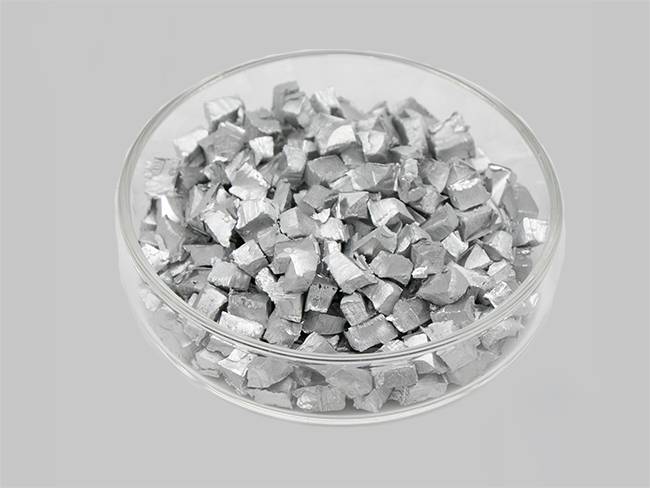
Rare precious metal targets, including platinum (Pt), ruthenium (Ru), and iridium (Ir), alongside special alloy targets, play a pivotal role in the fabrication of integrated circuit logic device chips. These materials are indispensable in the formation of high-performance metal films, which are essential for the intricate processes involved in semiconductor manufacturing.
<img alt="Rare and Precious Metals and Special Alloy Targets" class="lazy" data-src="data:image/jpeg;base64,/9j/4AAQSkZJRgABAQAAAQABAAD/4gHYSUNDX1BST0ZJTEUAAQEAAAHIAAAAAAQwAABtbnRyUkdCIFhZWiAH4AABAAEAAAAAAABhY3NwAAAAAAAAAAAAAAAAAAAAAAAAAAAAAAAAAAAAAQAA9tYAAQAAAADTLQAAAAAAAAAAAAAAAAAAAAAAAAAAAAAAAAAAAAAAAAAAAAAAAAAAAAAAAAAAAAAAAAAAAAlkZXNjAAAA8AAAACRyWFlaAAABFAAAABRnWFlaAAABKAAAABRiWFlaAAABPAAAABR3dHB0AAABUAAAABRyVFJDAAABZAAAAChnVFJDAAABZAAAAChiVFJDAAABZAAAAChjcHJ0AAABjAAAADxtbHVjAAAAAAAAAAEAAAAMZW5VUwAAAAgAAAAcAHMAUgBHAEJYWVogAAAAAAAAb6IAADj1AAADkFhZWiAAAAAAAABimQAAt4UAABjaWFlaIAAAAAAAACSgAAAPhAAAts9YWVogAAAAAAAA9tYAAQAAAADTLXBhcmEAAAAAAAQAAAACZmYAAPKnAAANWQAAE9AAAApbAAAAAAAAAABtbHVjAAAAAAAAAAEAAAAMZW5VUwAAACAAAAAcAEcAbwBvAGcAbABlACAASQBuAGMALgAgADIAMAAxADb/2wBDAAoHBwgHBgoICAgLCgoLDhgQDg0NDh0VFhEYIx8lJCIfIiEmKzcvJik0KSEiMEExNDk7Pj4+JS5ESUM8SDc9Pjv/2wBDAQoLCw4NDhwQEBw7KCIoOzs7Ozs7Ozs7Ozs7Ozs7Ozs7Ozs7Ozs7Ozs7Ozs7Ozs7Ozs7Ozs7Ozs7Ozs7Ozs7Ozv/wAARCAFWAcIDASIAAhEBAxEB/8QAHAABAQACAwEBAAAAAAAAAAAAAAEDBgIEBQcI/8QAPRAAAgEDAgQDBwMCAwcFAAAAAAECAwQRBSEGMQUhE2FxBxMigZGhsTLB0RQjFULhFiQlQ1Jy8DNEYrLC/8QAFgEBAQEAAAAAAAAAAAAAAAAAAAEC/8QAGBEBAQEBAQAAAAAAAAAAAAAAAAERITH/2gAMAwEAAhEDEQA/APpwHUAAAAKQAUAAAAAAAAAAAABQQAUAAAAAAAAAAAAAAIBQQAAAAAAAAAAAAAAAAAACAAAAAAAAAAAAAAAAAAAAAAAAACkAFAAAAAAAAAAAAAAAAKQAUgAAAAUAgFIUgAAAAAAAAAAAAAAAAAAACAAAAAAAAAAAAAAAAAAAAAAAAAAAAAKCAUAgAoAAAAAAAAAAAAAAAAAAAAAAAAAAAAAAAAAAAAAAAIAAAAAAAAAAAAAAgFBABQAAAAAAAAAAAAAAACkKAAAAAAAAAAAAAAAAAAAAAAAAAAAAAAAAAAAAAgFIAAAAAAAAAAAAAAAAAAAAAAAAAAAAFAAAAAAAgAAAAAAAAAAAFIUAAAAAAAAAAcZSUeu/YDkDE6zbwlgxvLe8mTR2HOK5tE97DuYGsEwhoz++gsc9/IKtB9TrpbNJhrk305k0dlTi+Ukck88jqpJIqbymm0dlTi+Ukck88jqpJIqbymm0dlTi+Ukck88jqpJIqbymm0dlTi+Ukck88jqpJIqbymm0dlTi+Ukck88jqpJIqbymm0dlTi+Ukck88jqpJIqbymm0dlTi+Ukck88jqpJIqbymm0dlTi+Ukck88jqpJIqbymm0dlTi+Ukck88jqpJIqbymm0dlTi+Ukck88jqpJIqbymm0dlTi+Ukck88jqpJIqbymm0dlTi+Ukck88jqpJIqbymm0dlTi+Ukck88jqpJIqbymm0dlTi+Ukck88jqpJIqbymm0dlTi+Ukck88jqpJIqbymm0dlTi+Ukck88jqpJIqbymm0dlTi+Ukck88jqpJIqbymm0dlTi+Ukck88jqpJIqbymm0dlTi+Ukck88jqpJIqbymm0dlTi+Ukck88jqpJIqbymm0dlTi+Ukck88jqpJIqbymm0dlTi+Ukck88jqpJIqbymm0dlTi+Ukck88jqpJIqbymm0dlTi+Ukck88jqpJIqbymm0dlTi+Ukck88jqpJIqbymm0dlTi+Ukck88jqpJIqbymm0dlTi+Ukck88jqpJIqbymm0dlTi+Ukck88jqpJIqbymm0dlTi+Ukck88jqpJIqbymm0dlTi+Ukck88jqpJIqbymm0dlTi+Ukck88jqpJIqbymm0dlTi+Ukck88jqpJIqbymm0dlTi+Ukck88jqpJIqbymm0dlTi+Ukck88jqpJIqbymm0dlTi+Ukck88jqpJIqbymm0dlTi+Ukck88jqpJIqbymm0dlTi+Ukck88jqpJIqbymm0dlTi+Ukck88jqpJIqbymm0dlTi+Ukck88jqpJIqbymm0dlTi+Ukck88jqpJIqbymm0dlTi+Ukck88jqpJIqbymm0dlTi+Ukck88jqpJIqbymm0dlTi+Ukck88jqpJIqbymm0dlTi+Ukck88jqpJIqbymm0dlTi+Ukck88jqpJIqbymm0dlTi+Ukck88jqpJIqbymm0dlTi+Ukck88jqpJIqbymm0dlTi+Ukck88jqpJIqbymm0dlTi+Ukck88jqpJIqbymm0dlTi+Ukck88jqpJIqbymm0dlTi+Ukck88jqpJIqbymm0dlTi+Ukck88jqpJIqbymm0dlTi+Ukck88jqpJIqbymm0dlTi+Ukck88jqpJIqbymm0dlTi+Ukck88jqpJIqbymm0dlTi+Ukck88jqpJIqbymm0dlTi+Ukck88jqpJIqbymm0dlTi+Ukck88jqpJIqbymm0dlTi+Ukck88jqpJIqbymm0dlTi+Ukck88jqpJIqbymm0dlTi+Ukck88jqpJIqbymm0dlTi+Ukck88jqpJIqbymm0dlTi+Ukck88jqpJIqbymm0dlTi+Ukck88jqpJIqbymm0dlTi+Ukck88jqpJIqbymm0dlTi+Ukck88jqpJIqbymm0dlTi+Ukck88jqpJIqbymm0dlTi+Ukck88jqpJIqbymm0dlTi+Ukck88jqpJIqbymm0dlTi+Ukck88jqpJIqbymm0dlTi+Ukck88jqpJIqbymm0dlTi+Ukck88jqpJIqbymm0dlTi+Ukck88jqpJIqbymm0dlTi+Ukck88jqpJIqbymm0dlTi+Ukck88jqpJIqbymm0dlTi+Ukck88jqpJIqbymm0dlTi+Ukck88jqpJIqbymm0dlTi+Ukck88jqpJIqbymm0dlTi+Ukck88jqpJIqbymm0dlTi+Ukck88jqpJIqbymm0dlTi+Ukck88jqpJIqbymm0dlTi+Ukck88jqpJIqbymm0dlTi+Ukck88jqpJIqbymm0dlTi+Ukck88jqpJIqbymm0dlTi+Ukck88jqpJIqbymm0dlTi+Ukck88jqpJIqbymm0dlTi+Ukck88jqpJIqbymm0dlTi+Ukck88jqpJIqbymm0dlTi+Ukck88jqpJIqbymm0dlTi+Ukck88jqpJIqbymm0dlTi+Ukck88jqpJIqbymm0dlTi+Ukck88jqpJIqbymm0dlTi+Ukck88jqpJIqbymm0dlTi+Ukck88jqpJIqbymm0dlTi+Ukck88jqpJIqbymm0dlTi+Ukck88jqpJIqbymm0dlTi+Ukck88jqpJIqbymm0dlTi+Ukck88jqpJIqbymm0dlTi+Ukck88jqpJIqbymm0dlTi+Ukck88jqpJIqbymm0dlTi+Ukck88jqpJIqbymm0dlTi+Ukck88jqpJIqbymm0dlTi+Ukck88jqpJIqbymm0dlTi+Ukck88jqpJIqbymm0dlTi+Ukck88jqpJIqbymm0dlTi+Ukck88jqpJIqbymm0dlTi+Ukck88jqpJIqbymm0dlTi+Ukck88jqpJIqbymm0dlTi+Ukck88jqpJIqbymm0dlTi+Ukck88jqpJIqbymm0dlTi+Ukck88jqpJIqbymm0dlTi+Ukck88jqpJIqbymm0dlTi+Ukck88jqpJIqbymm0dlTi+Ukck88jqpJIqbymm0dlTi+Ukck88jqpJIqbymm0dlTi+Ukck88jqpJIqbymm0dlTi+Ukck88jqpJIqbymm0dlTi+Ukck88jqpJIqbymm0dlTi+Ukck88jqpJIqbymm0dlTi+Ukck88jqpJIqbymm0dlTi+Ukck88jqpJIqbymm0dlTi+Ukck88jqpJIqbymm0dlTi+Ukck88jqpJIqbymm0dlTi+Ukck88jqpJIqbymm0dlTi+Ukck88jqpJIqbymm0dlTi+Ukck88jqpJIqbymm0dlTi+Ukck88jqpJIqbymm0dlTi+Ukck88jqpJIqbymm0dlTi+Ukck88jqpJIqbymm0dlTi+Ukck88jqpJIqbymm0dlTi+Ukck88jqpJIqbymm0dlTi+Ukck88jqpJIqbymm0dlTi+Ukck88jqpJIqbymm0dlTi+Ukck88jqpJIqbymm0dlTi+Ukck88jqpJIqbymm0dlTi+Ukck88jqpJIqbymm0dlTi+Ukck88jqpJIqbymm0dlTi+Ukck88jqpJIqbymm0dlTi+Ukck88jqpJIqbymm0dlTi+Ukck88jqpJIqbymm0dlTi+Ukck88jqpJIqbymm0dlTi+Ukck88jqpJIqbymm0dlTi+Ukck88jqpJIqbymm0dlTi+Ukck88jqpJIqbymm0dlTi+Ukck88jqpJIqbymm0dlTi+Ukck88jqpJIqbymm0dlTi+Ukck88jqpJIqbymm0dlTi+Ukck88jqpJIqbymm0dlTi+Ukck88jqpJIqbymm0dlTi+Ukck88jqpJIqbymm0dlTi+Ukck88jqpJIqbymm0dlTi+Ukck88jqpJIqbymm0dlTi+Ukck88jqpJIqbymm0dlTi+Ukck88jqpJIqbymm0dlTi+Ukck88jqpJIqbymm0dlTi+Ukck88jqpJIqbymm0dlTi+Ukck88jqpJIqbymm0dlTi+Ukck88jqpJIqbymm0dlTi+Ukck88jqpJIqbymm0dlTi+Ukck88jqpJIqbymm0dlTi+Ukck88jqpJIqbymm0dlTi+Ukck88jqpJIqbymm0dlTi+Ukck88jqpJIqbymm0dlTi+Ukck88jqpJIqbymm0dlTi+Ukck88jqpJIqbymm0dlTi+Ukck88jqpJIqbymm0dlTi+Ukck88jqpJIqbymm0dlTi+Ukck88jqpJIqbymm0dlTi+Ukck88jqpJIqbymm0dlTi+Ukck88jqpJIqbymm0dlTi+Ukck88jqpJIqbymm0dlTi+Ukck88jqpJIqbymm0dlTi+Ukck88jqpJIqbymm0dlTi+Ukck88jqpJIqbymm0dlTi+Ukck88jqpJIqbymm0dlTi+Ukck88jqpJIqbymm0dlTi+Ukck88jqpJIqbymm0dlTi+Ukck88jqpJIqbymm0dlTi+Ukck88jqpJIqbymm0dlTi+Ukck88jqpJIqbymm0dlTi+Ukck88jqpJIqbymm0dlTi+Ukck88jqpJIqbymm0dlTi+Ukck88jqpJIqbymm0dlTi+Ukck88jqpJIqbymm0dlTi+Ukck88jqpJIqbymm0dlTi+Ukck88jqpJIqbymm0dlTi+Ukck88jqpJIqbymm0dlTi+Ukck88jqpJIqbymm0dlTi+Ukck88jqpJIqbymm0dlTi+Ukck88jqpJIqbymm0dlTi+Ukck88jqpJIqbymm0dlTi+Ukck88jqpJIqbymm0dlTi+Ukck88jqpJIqbymm0dlTi+Ukck88jqpJIqbymm0dlTi+Ukck88jqpJIqbymm0dlTi+Ukck88jqpJIqbymm0dlTi+Ukck88jqpJIqbymm0dlTi+Ukck88jqpJIqbymm0dlTi+Ukck88jqpJIqbymm0dlTi+Ukck88jqpJIqbymm0dlTi+Ukck88jqpJIqbymm0dlTi+Ukck88jqpJIqbymm0dlTi+Ukck88jqpJIqbymm0dlTi+Ukck88jqpJIqbymm0dlTi+Ukck88jqpJIqbymm0dlTi+Ukck88jqpJIqbymm0dlTi+Ukck88jqpJIqbymm0dlTi+Ukck88jqpJIqbymm0dlTi+Ukck88jqpJIqbymm0dlTi+Ukck88jqpJIqbymm0dlTi+Ukck88jqpJIqbymm0dlTi+Ukck88jqpJIqbymm0dlTi+Ukck88jqpJIqbymm0dlTi+Ukck88jqpJIqbymm0dlTi+Ukck88jqpJIqbymm0dlTi+Ukck88jqpJIqbymm0dlTi+Ukck88jqpJIqbymm0dlTi+Ukck88jqpJIqbymm0dlTi+Ukck88jqpJIqbymm0dlTi+Ukck88jqpJIqbymm0dlTi+Ukck88jqpJIqbymm0dlTi+Ukck88jqpJIqbymm0dlTi+Ukck88jqpJIqbymm0dlTi+Ukck88jqpJIqbymm0dlTi+Ukck88jqpJIqbymm0dlTi+Ukck88jqpJIqbymm0dlTi+Ukck88jqpJIqbymm0dlTi+Ukck88jqpJIqbymm0dlTi+Ukck88jqpJIqbymm0dlTi+Ukck88jqpJIqbymm0dlTi+Ukck88jqpJIqbymm0dlTi+Ukck88jqpJIqbymm0dlTi+Ukck88jqpJIqbymm0dlTi+Ukck88jqpJIqbymm0dlTi+Ukck88jqpJIqbymm0dlTi+Ukck88jqpJIqbymm0dlTi+Ukck88jqpJIqbymm0dlTi+Ukck88jqpJIqbymm0dlTi+Ukck88jqpJIqbymm0dlTi+Ukck88jqpJIqbymm0dlTi+Ukck88jqpJIqbymm0dlTi+Ukck88jqpJIqbymm0dlTi+Ukck88jqpJIqbymm0dlTi+Ukck88jqpJIqbymm0dlTi+Ukck88jqpJIqbymm0dlTi+Ukck88jqpJIqbymm0dlTi+Ukck88jqpJIqbymm0dlTi+Ukck88jqpJIqbymm0dlTi+Ukck88jqpJIqbymm0dlTi+Ukck88jqpJIqbymm0dlTi+Ukck88jqpJIqbymm0dlTi+Ukck88jqpJIqbymm0dlTi+Ukck88jqpJIqbymm0dlTi+Ukck88jqpJIqbymm0dlTi+Ukck88jqpJIqbymm0dlTi+Ukck88jqpJIqbymm0dlTi+Ukck88jqpJIqbymm0dlTi+Ukck88jqpJIqbymm0dlTi+Ukck88jqpJIqbymm0dlTi+Ukck88jqpJIqbymm0dlTi+Ukck88jqpJIqbymm0dlTi+Ukck88jqpJIqbymm0dlTi+Ukck88jqpJIqbymm0dlTi+Ukck88jqpJIqbymm0dlTi+Ukck88jqpJIqbymm0dlTi+Ukck88jqpJIqbymm0dlTi+Ukck88jqpJIqbymm0dlTi+Ukck88jqpJIqbymm0dlTi+Ukck88jqpJIqbymm0dlTi+Ukck88jqpJIqbymm0dlTi+Ukck88jqpJIqbymm0dlTi+Ukck88jqpJIqbymm0dlTi+Ukck88jqpJIqbymm0dlTi+Ukck88jqpJIqbymm0dlTi+Ukck88jqpJIqbymm0dlTi+Ukck88jqpJIqbymm0dlTi+Ukck88jqpJIqbymm0dlTi+Ukck88jqpJIqbymm0dlTi+Ukck88jqpJIqbymm0dlTi+Ukck88jqpJIqbymm0dlTi+Ukck88jqpJIqbymm0dlTi+Ukck88jqpJIqbymm0dlTi+Ukck88jqpJIqbymm0dlTi+Ukck88jqpJIqbymm0dlTi+Ukck88jqpJIqbymm0dlTi+Ukck88jqpJIqbymm0dlTi+Ukck88jqpJIqbymm0dlTi+Ukck88jqpJIqbymm0dlTi+Ukck88jqpJIqbymm0dlTi+Ukck88jqpJIqbymm0dlTi+Ukck88jqpJIqbymm0dlTi+Ukck88jqpJIqbymm0dlTi+Ukck88jqpJIqbymm0dlTi+Ukck88
Related Products
- High Purity Pure Graphite Crucible for Electron Beam Evaporation
- High Purity Pure Graphite Crucible for Evaporation
- High Purity Alumina Granulated Powder for Engineering Advanced Fine Ceramics
Related Articles
- Electron Beam Evaporation Coating: Advantages, Disadvantages, and Applications
- Why Your Graphite Components Keep Failing—And How to Stop It for Good
- Electron Beam Evaporation Technology in Vacuum Coating
- The Role and Types of Crucibles in Scientific Experiments
- Electron Beam Evaporation Coating Technology and Material Selection