
Overview of Magnetron Sputtering
Role of Target Material
The target material plays a pivotal role in the deposition quality of thin films during wafer manufacturing. This material, often referred to as the sputtering target, is subjected to high-energy particles that cause atoms to be ejected from its surface. These atoms then migrate and condense on the wafer substrate, forming a thin film. The characteristics of the target material directly influence the properties of the deposited film, including its electrical conductivity, optical transparency, and mechanical durability.
For instance, the purity of the target material is paramount. Any impurities in the target can lead to defects in the film, affecting its overall performance. Similarly, the density of the target material is crucial for ensuring a uniform sputtering rate, which in turn affects the thickness and consistency of the deposited film. Additionally, the grain size of the target material can impact the film's uniformity and reduce the likelihood of defects, thereby enhancing the quality of the final product.
In summary, the target material is not merely a passive component in the sputtering process; it is an active determinant of the quality and performance of the thin films produced in wafer manufacturing.
Sputtering Process
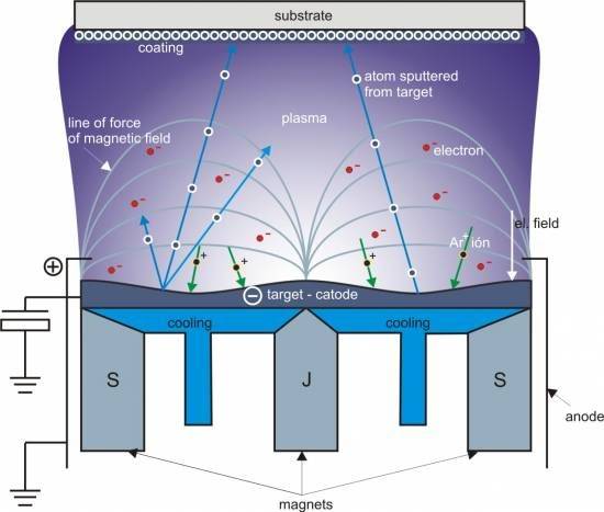
The sputtering process involves high-speed argon ions bombarding a target material, causing atoms or molecules to be ejected from the surface. These ejected particles then migrate towards a wafer substrate where they coalesce to form a thin film. This method is a cornerstone of thin-film deposition techniques, particularly within the realm of Physical Vapor Deposition (PVD) processes.
During sputtering, the energetic ions, primarily noble gas ions, impinge upon the target material. This bombardment imparts sufficient energy to dislodge atoms from the target's solid state into the gas phase. The liberated atoms subsequently travel through the vacuum environment and settle onto the substrate, where they assemble into a coherent film.
Sputtering is not only utilized for coating applications but also serves as a critical tool in surface physics. It is employed for preparing high-purity surfaces and for analyzing the chemical composition of surfaces. The process leverages the energy of a plasma, a partially ionized gas, which acts upon the target's surface to extract material atoms one by one, ensuring precise and controlled deposition onto the substrate.
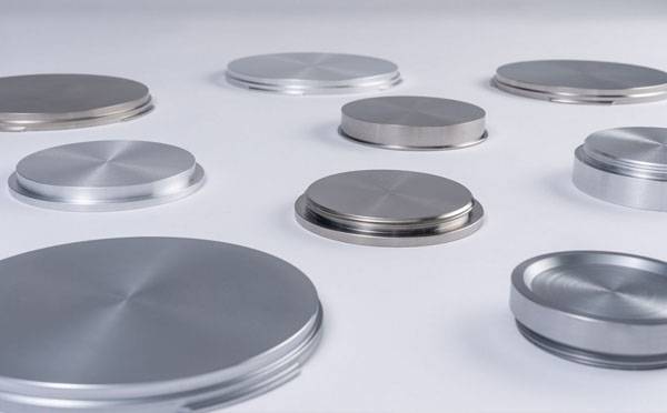
Types of Sputtering Targets
Monolithic Targets
Monolithic targets are a critical component in the sputtering process, playing a pivotal role in the deposition of thin films. These targets are composed of single materials, which can be broadly categorized into two main groups: metal single targets and non-metallic monomers.
Metal single targets are typically made from materials such as aluminum (Al), copper (Cu), and silver (Ag). These metals are chosen for their excellent electrical conductivity, thermal stability, and the ability to form high-quality thin films. For instance, aluminum is widely used in the production of reflective coatings and interconnects in microelectronics due to its high reflectivity and low resistivity.
On the other hand, non-metallic monomers include elements like selenium (Se), silicon (Si), and boron (B). These materials are selected for their unique properties that are essential for specific applications. Selenium, for example, is often used in the production of photoconductive layers in imaging devices, while silicon is crucial in the fabrication of semiconductor devices.
The selection of monolithic targets is not arbitrary; it is driven by the specific requirements of the thin film being deposited. Each material has its own set of characteristics that influence the final properties of the film, such as its electrical, optical, and mechanical performance. Therefore, understanding the nuances of each target material is essential for achieving the desired outcomes in wafer manufacturing.
In summary, monolithic targets offer a versatile and effective solution for various sputtering applications, thanks to their single-material composition and the tailored properties they bring to the deposition process.
Composite Targets
Composite sputtering targets encompass a diverse array of materials, each tailored to specific applications in thin film deposition. These targets include borides, cemented carbides, nitrides, selenides, silicides, sulfides, arsenides, and oxides. Each type of composite target offers unique properties that influence the characteristics of the deposited film.
- Borides: Known for their high hardness and thermal stability, boride targets are often used in applications requiring wear-resistant coatings.
- Cemented Carbides: Comprising a binder metal (usually cobalt) and hard ceramic particles (such as tungsten carbide), these targets provide excellent resistance to abrasion and high-temperature performance.
- Nitrides: Characterized by their extreme hardness and chemical inertness, nitride targets are frequently employed in the production of cutting tools and decorative coatings.
- Selenides: Offering unique optical properties, selenide targets are crucial in the fabrication of optoelectronic devices and solar cells.
- Silicides: With their excellent electrical conductivity and thermal stability, silicide targets are essential in semiconductor manufacturing for creating contacts and interconnects.
- Sulfides: Known for their lubricity and optical properties, sulfide targets are used in applications such as anti-friction coatings and infrared optics.
- Arsenides: Providing high electron mobility, arsenide targets are vital in the production of high-speed electronic devices and photovoltaic cells.
- Oxides: Renowned for their electrical, optical, and magnetic properties, oxide targets are extensively used in the fabrication of capacitors, resistors, and magnetic storage devices.
Each of these composite targets plays a critical role in achieving the desired film properties, ensuring the functionality and performance of the final product.
Key Parameters for Sputtering Targets
Purity
The purity of sputtering targets is a critical factor that directly influences the quality of the thin films produced. To achieve optimal electrical, optical, and mechanical properties in the deposited films, targets must be exceptionally pure. Impurities can lead to defects such as voids, inclusions, and non-uniformities, which can significantly degrade the performance of the final product.
For instance, high-purity targets ensure that the deposited films exhibit superior conductivity, transparency, and mechanical strength. This is particularly important in applications such as semiconductor manufacturing, where even trace amounts of impurities can result in device failure. The purity requirements are often stringent, with many industries specifying targets with impurity levels below parts per million (ppm).
| Impurity Source | Potential Impact |
|---|---|
| Metallic Contaminants | Reduced conductivity, increased resistance |
| Non-metallic Inclusions | Optical distortions, mechanical weakness |
| Oxide Layers | Reduced adhesion, film delamination |
Achieving such high levels of purity involves rigorous manufacturing processes, including advanced purification techniques and stringent quality control measures. These processes ensure that the target material is free from contaminants that could compromise the integrity of the thin films.
Density
Higher density targets are crucial for maintaining a uniform sputtering rate and extending the service life of the target material. The density of a sputtering target directly influences the efficiency and consistency of the sputtering process, which is essential for the deposition of high-quality thin films in wafer manufacturing.
A denser target material ensures that the high-speed argon ions, which are responsible for sputtering atoms or molecules from the target, interact more uniformly with the surface. This uniform interaction leads to a more consistent deposition rate, which is vital for achieving the desired film properties such as electrical conductivity, optical transparency, and mechanical strength.
Moreover, higher density targets tend to have a longer service life due to their ability to withstand the intense bombardment of ions without significant degradation. This durability is particularly important in industrial applications where frequent target replacements can be costly and time-consuming.
In summary, the density of a sputtering target is a critical parameter that impacts both the efficiency of the sputtering process and the longevity of the target material, making it a key consideration in the selection and design of sputtering targets.
Grain Size
Smaller grain size in sputtering targets plays a pivotal role in enhancing the quality of the deposited thin films. This parameter directly influences the number of defects present in the film, which can significantly impact the performance and reliability of the final product.
Impact on Defect Reduction
The reduction in grain size leads to a more uniform distribution of atoms during the sputtering process. This uniformity minimizes the formation of voids, cracks, and other structural imperfections that can act as defect sites. As a result, the film's mechanical integrity is improved, making it more resistant to stress and deformation.
Improvement in Film Uniformity
A finer grain structure allows for better control over the deposition process, leading to more consistent film thickness across the wafer. This uniformity is crucial for applications where precise film properties are necessary, such as in semiconductor manufacturing. The smoother surface achieved with smaller grain sizes also reduces the likelihood of surface irregularities that could affect the film's optical and electrical properties.
Practical Implications
In practical terms, targets with smaller grain sizes are often preferred in high-precision applications where the quality of the thin film is paramount. This preference is evident in industries such as microelectronics, where even minor defects can lead to significant performance issues. The use of targets with optimized grain size ensures that the resulting films meet the stringent quality standards required for these advanced applications.
Related Products
- Reference Electrode Calomel Silver Chloride Mercury Sulfate for Laboratory Use
- Multifunctional Electrolytic Electrochemical Cell Water Bath Single Layer Double Layer
- Molybdenum Tungsten Tantalum Special Shape Evaporation Boat
- Hemispherical Bottom Tungsten Molybdenum Evaporation Boat
- Cylindrical Press Mold with Scale for Lab
Related Articles
- Pseudo-Reference Electrodes When and How to Use Them
- Common Reference Electrodes in Electrochemical Studies
- A Comprehensive Guide to Reference Electrodes
- A Beginner's Guide to Understanding Reference Electrodes in Electrochemistry
- Comprehensive Guide to Reference Electrodes: Types, Applications, and Selection Criteria


