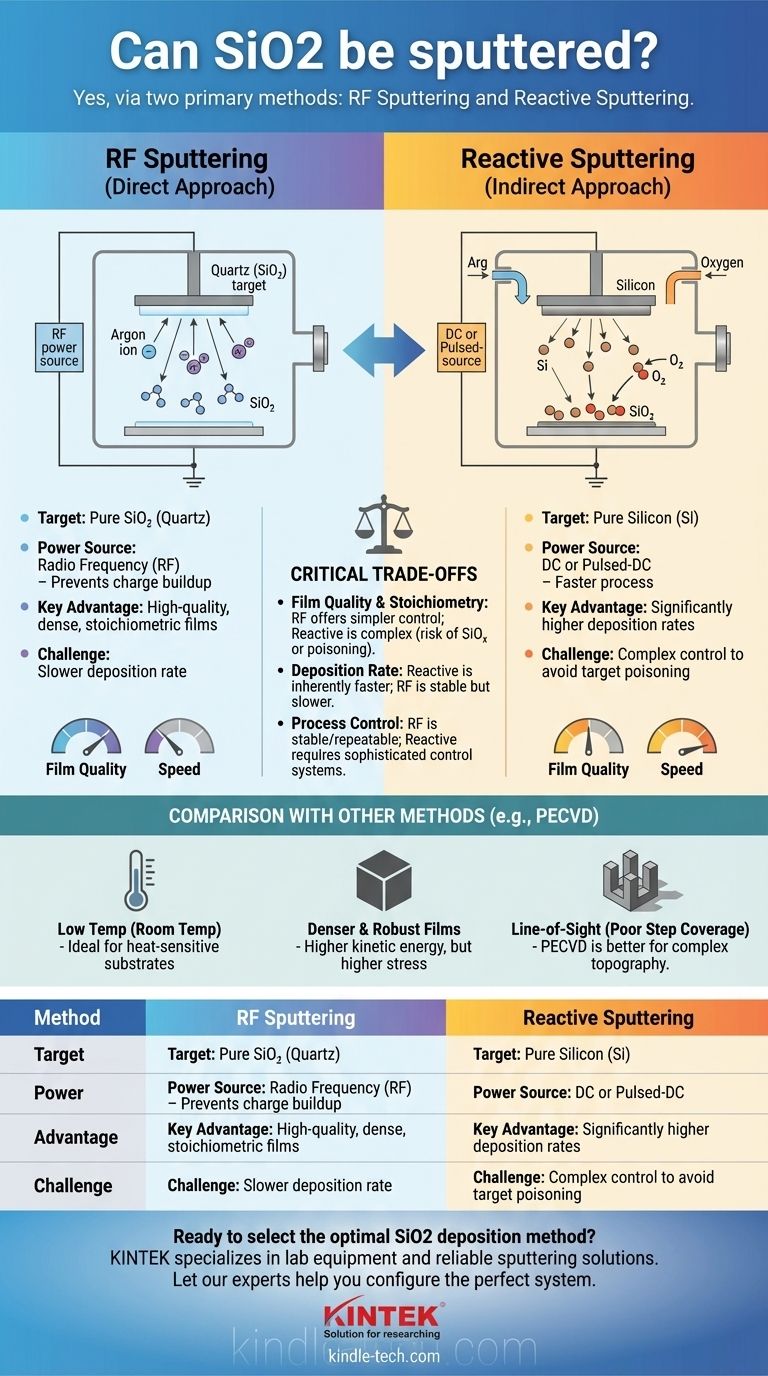
Yes, silicon dioxide (SiO2) is routinely deposited using sputtering, a standard physical vapor deposition (PVD) technique. The process can be accomplished via two primary methods: directly sputtering from a silicon dioxide target using radio frequency (RF) power, or reactively sputtering from a pure silicon target in an oxygen-rich environment.
The question is not whether you can sputter SiO2, but which method is appropriate for your goals. The choice between direct RF sputtering and reactive sputtering involves a critical trade-off between film quality, process simplicity, and deposition speed.
The Two Primary Sputtering Methods for SiO2
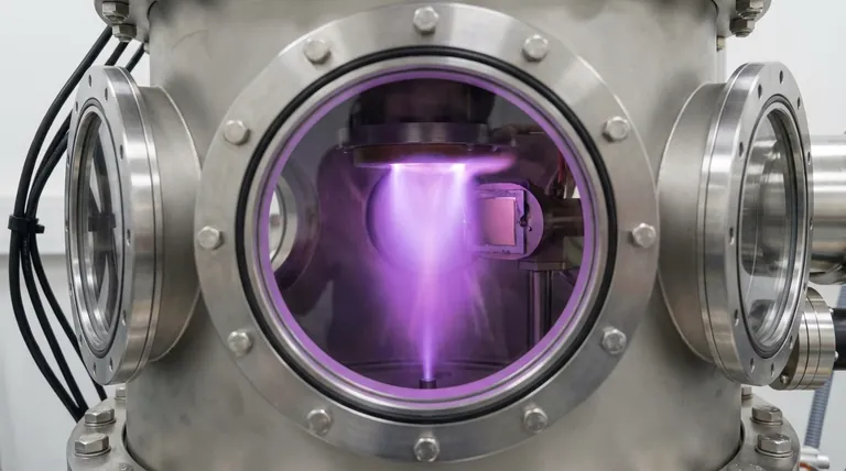
Sputtering is a process where atoms are ejected from a solid target material after it is bombarded by energetic ions from a plasma. For SiO2, the implementation depends on the nature of that target.
RF Sputtering: The Direct Approach
This method uses a target made of pure silicon dioxide (quartz). Because SiO2 is an excellent electrical insulator, a standard direct current (DC) power source cannot be used.
Applying a negative DC voltage would cause positive ions (like Argon) to bombard the target, but the insulating surface would quickly accumulate a positive charge, repelling further ions and stopping the process.
Radio Frequency (RF) sputtering solves this by alternating the voltage at high frequency. During the negative cycle, ions sputter the target, and during the positive cycle, electrons are attracted to the surface to neutralize the charge buildup, allowing the process to continue indefinitely.
This method is known for producing high-quality, dense, and stoichiometric SiO2 films with excellent insulating properties.
Reactive Sputtering: The Indirect Approach
Reactive sputtering uses a target made of pure, conductive (or semi-conductive) silicon. Because the target is conductive, a simpler and often faster DC or pulsed-DC power source can be used.
In this process, silicon atoms are sputtered from the target into a vacuum chamber containing a mixture of an inert gas (like Argon) and a reactive gas (Oxygen).
The sputtered silicon atoms react with the oxygen—either in transit or on the substrate surface—to form a silicon dioxide film. This technique can achieve significantly higher deposition rates than RF sputtering.
Understanding the Trade-offs
Choosing the right sputtering method requires you to balance several competing factors. Your application's requirements will dictate which trade-offs are acceptable.
Film Quality and Stoichiometry
RF sputtering generally offers more straightforward control over film quality. Since you are sputtering the desired material directly, achieving the correct Si:O atomic ratio (stoichiometry) is relatively simple, resulting in highly reliable insulating films.
Reactive sputtering is more complex. You must precisely balance the silicon sputtering rate with the oxygen gas flow. Too little oxygen results in a silicon-rich, absorptive film (SiOx, where x<2) with poor dielectric properties. Too much oxygen can "poison" the silicon target by forming an insulating SiO2 layer on its surface, causing a dramatic drop in the sputtering rate.
Deposition Rate vs. Process Control
The primary advantage of reactive sputtering is its potential for high throughput. Sputtering from a metallic silicon target is inherently faster than sputtering from a ceramic SiO2 target.
However, this speed comes at the cost of complexity. Maintaining a stable process window to avoid target poisoning requires sophisticated control of power and gas flow, often involving feedback loops.
RF sputtering is typically slower but offers a more stable and repeatable process, making it ideal for research or applications where quality is more critical than speed.
Sputtering vs. Other Deposition Methods (e.g., PECVD)
It is also critical to compare sputtering to alternative deposition techniques like Plasma-Enhanced Chemical Vapor Deposition (PECVD).
- Temperature: Sputtering is a physical process that can be performed at or near room temperature. This makes it ideal for depositing onto temperature-sensitive substrates like plastics or pre-processed devices. PECVD is a chemical process that requires higher temperatures (typically 200-400°C) to drive the necessary reactions.
- Film Density & Stress: Sputtered films are generally denser and more robust because the sputtered atoms have higher kinetic energy upon arrival at the substrate. However, this can also lead to higher intrinsic film stress.
- Step Coverage: Sputtering is a line-of-sight process, which can lead to poor coverage on complex 3D structures (shadowing). PECVD offers superior conformal coating (step coverage) because the precursor gases can flow around features before reacting on the surface.
Making the Right Choice for Your Goal
Your decision must be driven by your project's most critical parameter, whether it's film quality, deposition speed, or substrate compatibility.
- If your primary focus is the highest electrical insulation and process simplicity: Choose RF sputtering from a quartz target for its reliable stoichiometry and stability.
- If your primary focus is high-volume manufacturing and throughput: Use reactive sputtering from a silicon target, but be prepared to invest resources in process development and control.
- If your primary focus is coating complex topography with high aspect ratios: Consider alternatives like PECVD for its superior conformal coverage.
- If your primary focus is depositing on heat-sensitive materials: Sputtering is an excellent choice due to its fundamentally low-temperature nature.
By understanding these core principles and trade-offs, you can confidently select the right deposition strategy for your specific application.
Summary Table:
| Method | Target Material | Power Source | Key Advantage | Key Challenge |
|---|---|---|---|---|
| RF Sputtering | SiO2 (Quartz) | Radio Frequency (RF) | High-quality, stoichiometric films | Slower deposition rate |
| Reactive Sputtering | Silicon (Si) | DC or Pulsed-DC | High deposition rate, faster process | Complex process control to avoid target poisoning |
Ready to select the optimal SiO2 deposition method for your project? The choice between RF and reactive sputtering is critical for achieving the right balance of film quality, speed, and process control for your specific application. KINTEK specializes in lab equipment and consumables, serving laboratory needs with expert advice and reliable sputtering solutions. Let our experts help you configure the perfect system to meet your research or production goals. Contact us today to discuss your requirements!
Visual Guide
Related Products
- Spark Plasma Sintering Furnace SPS Furnace
- Chemical Vapor Deposition CVD Equipment System Chamber Slide PECVD Tube Furnace with Liquid Gasifier PECVD Machine
People Also Ask
- What is the mechanism of SPS process? A Deep Dive into Rapid, Low-Temperature Sintering
- What is the process fundamentals of spark plasma sintering? Achieve Rapid, High-Density Material Consolidation
- What are the fundamentals of spark plasma sintering process? Unlock Rapid, High-Performance Material Consolidation
- What is SPS sintering method? A Guide to High-Speed, High-Performance Material Fabrication
- What are the advantages of CAMI/SPS for W-Cu composite preparation? Reduce cycles from hours to seconds.

