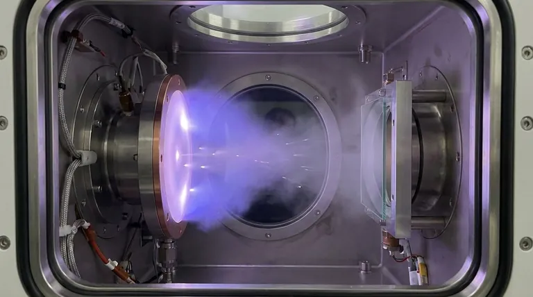
At its core, a sputtering target is the source material used to create an ultra-thin film on another object. It is a precisely engineered slab of pure metal, alloy, or ceramic compound that is placed in a vacuum chamber. During the sputtering process, this target is bombarded with high-energy ions, which physically knock atoms off its surface, vaporizing the material so it can be deposited elsewhere as a coating.
A sputtering target is not merely a block of material; it is the foundational component in a sophisticated coating process. The quality, purity, and structure of the target directly dictate the performance and integrity of the final thin film deposited on a product.
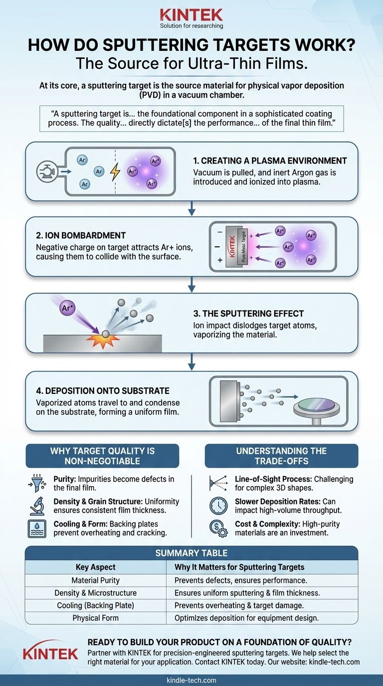
The Sputtering Process: From Solid Target to Thin Film
To understand how a sputtering target works, you must first understand the environment it operates in. The entire process, known as Physical Vapor Deposition (PVD), takes place inside a high-vacuum chamber.
Step 1: Creating a Plasma Environment
The process begins by pumping nearly all the air out of the chamber to create a vacuum. This ensures the vaporized atoms from the target can travel to their destination without colliding with air molecules.
Next, a small amount of an inert gas, typically Argon (Ar), is introduced into the chamber.
Step 2: Ion Bombardment
A high voltage is applied within the chamber, which strips electrons from the Argon gas atoms, turning them into positively charged ions (Ar+). This cloud of ionized gas is called a plasma.
The sputtering target itself is given a strong negative charge, causing it to act as a cathode. This powerful negative charge aggressively attracts the positively charged Argon ions, causing them to accelerate and collide with the target's surface at high velocity.
Step 3: The "Sputtering" Effect
This high-energy ionic bombardment is the heart of the process. When an Argon ion strikes the target, its kinetic energy is transferred to the target material, physically dislodging or "sputtering" individual atoms from the surface.
These ejected atoms are now a fine vapor that travels through the vacuum chamber.
Step 4: Deposition onto the Substrate
The object to be coated, known as the substrate, is strategically placed within the chamber. The vaporized atoms from the target travel in a straight line until they strike the substrate's surface.
Upon arrival, they condense and build up, layer by layer, forming a thin, highly uniform, and tightly bonded film.
Why Target Quality is Non-Negotiable
The sputtering process is a direct transfer of material from the target to the substrate. This means that any flaw or imperfection in the target will be replicated in the final coating, making target quality a critical factor.
The Role of Purity
A sputtering target must have extremely high purity. Any impurity atoms within the target will be sputtered along with the desired material, becoming contaminants in the final film and compromising its electrical, optical, or mechanical properties.
Importance of Density and Grain Structure
A target with low density or internal voids will sputter unevenly and can release trapped gases, causing defects in the coating. A uniform, fine-grained microstructure ensures a stable and consistent sputtering rate, leading to a film of predictable thickness and quality.
Physical Form and Cooling
Sputtering generates significant heat. Targets are bonded to a metallic holder, called a backing plate, which contains channels for water cooling. This prevents the target from overheating, cracking, or melting during the process.
The target's shape—whether a simple flat disc or a more complex cylindrical or ring shape—is determined by the design of the sputtering equipment.
Understanding the Trade-offs
While powerful, the sputtering process has inherent characteristics that make it suitable for some applications more than others.
Sputtering is a Line-of-Sight Process
The sputtered atoms travel in a straight line from the target to the substrate. This makes it challenging to uniformly coat complex, three-dimensional shapes with shadowed areas or deep recesses.
Deposition Rates Can Be Slow
Compared to other methods like thermal evaporation, sputtering can be a slower process. This can impact throughput in high-volume manufacturing, though it often provides superior film quality and adhesion.
Target Cost and Complexity
High-purity materials and the complex manufacturing required to achieve the right density and grain structure make high-quality sputtering targets a significant cost factor. Targets made from rare materials or complex alloys are particularly expensive.
Making the Right Choice for Your Goal
The specific requirements for a sputtering target are dictated entirely by the intended application of the final thin film.
- If your primary focus is cutting-edge electronics: Absolute purity and microstructural uniformity are paramount to create reliable semiconductor circuits or data storage layers.
- If your primary focus is durable mechanical tools: The target material must provide hardness and wear resistance, leading to the use of ceramic or carbide targets like TiC and BN.
- If your primary focus is large-area coating (like architectural glass): Cost-effectiveness, target lifespan, and a high, stable deposition rate are the key drivers for material selection.
Ultimately, the sputtering target is the origin of your coating, and its precise composition is the foundation for the performance of your final product.
Summary Table:
| Key Aspect | Why It Matters for Sputtering Targets |
|---|---|
| Material Purity | Impurities become defects in the final film, compromising performance. |
| Density & Microstructure | Ensures uniform sputtering and consistent film thickness. |
| Cooling (Backing Plate) | Prevents target overheating, cracking, and melting during the process. |
| Physical Form | Matches the sputtering equipment design for optimal deposition. |
Ready to build your product on a foundation of quality?
The performance of your thin film—whether for advanced semiconductors, durable cutting tools, or energy-efficient glass—starts with the sputtering target. At KINTEK, we specialize in providing high-purity lab equipment and consumables, including precision-engineered sputtering targets. Our targets are manufactured to meet the exacting demands of your specific application, ensuring superior film quality, consistency, and adhesion.
Let our experts help you select the right target material and configuration to achieve your goals. Contact KINTEK today to discuss your project and discover how our solutions can enhance your coating process.
Visual Guide
Related Products
- Reference Electrode Calomel Silver Chloride Mercury Sulfate for Laboratory Use
- Multifunctional Electrolytic Electrochemical Cell Water Bath Single Layer Double Layer
- Molybdenum Tungsten Tantalum Special Shape Evaporation Boat
- Hemispherical Bottom Tungsten Molybdenum Evaporation Boat
- Cylindrical Press Mold with Scale for Lab
People Also Ask
- Which type of electrode can be used as a reference point? Select the Right One for Accurate Measurements
- What is the reference electrode in potentiometry? The Key to Stable & Accurate Measurements
- Which electrode is used as a reference electrode for measuring half-cell potentials? Understanding the Universal Standard
- Which electrode is used as a reference? A Guide to Accurate Electrochemical Measurements
- Why is the selection of a high-quality reference electrode critical in the electrochemical synthesis? | KINTEK


