The primary benefits of RF sputtering are its unique ability to deposit insulating materials, its enhanced process stability that prevents destructive arcing, and its efficiency in creating high-quality, uniform thin films at lower operating pressures. This combination of features makes it an exceptionally versatile and reliable thin-film deposition technique.
RF sputtering solves the fundamental limitation of DC sputtering by using an alternating electric field. This prevents catastrophic charge buildup on insulating targets, enabling the deposition of virtually any material—from metals to ceramics—with superior stability and film quality.
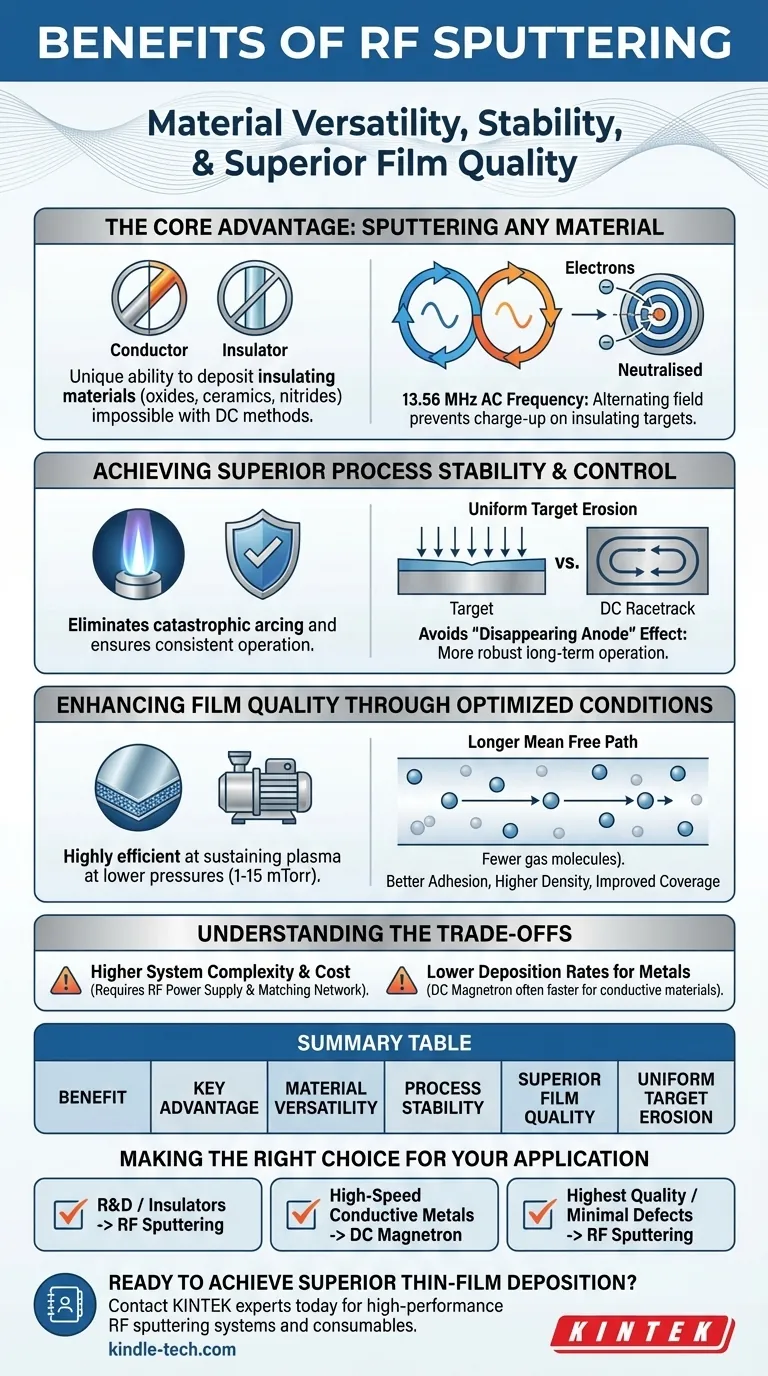
The Core Advantage: Sputtering Any Material
The single most important benefit of Radio Frequency (RF) sputtering is its material versatility. It opens the door to depositing films that are impossible to create with simpler direct current (DC) methods.
Overcoming the Insulator Challenge
In standard DC sputtering, a negative voltage is applied to the target material. This requires the target to be electrically conductive to complete the circuit and sustain the process.
If you attempt to use a non-conductive (insulating) target, positive ions from the plasma build up on its surface. This "charge-up" effect quickly neutralizes the negative potential, extinguishing the plasma and stopping the deposition process.
How the Alternating Field Works
RF sputtering replaces the constant DC voltage with a high-frequency alternating current (typically 13.56 MHz). During one half of the AC cycle, the target is bombarded by positive ions, sputtering material away as intended.
During the other half-cycle, the target becomes positive, attracting a flood of highly mobile electrons from the plasma. This instantly neutralizes the positive charge that built up, effectively "resetting" the target surface millions of time per second and allowing the process to continue indefinitely.
Unlocking Material Possibilities
This mechanism makes RF sputtering the go-to method for depositing a vast range of materials that are off-limits to DC sputtering. This includes critical materials like oxides (e.g., SiO₂), nitrides (e.g., Si₃N₄), ceramics, and various composites.
Achieving Superior Process Stability and Control
The use of an AC source not only enables insulator deposition but also creates a fundamentally more stable and controllable process, resulting in higher-quality films.
Eliminating Arcs and Charge-Up
The constant charge neutralization inherent to RF sputtering dramatically reduces or eliminates arcing. Arcing is a common failure mode in sputtering where localized charge buildup leads to a sudden, high-current discharge that can damage the target and create defects in the growing film.
Ensuring Uniform Target Erosion
Many sputtering systems use magnets to confine the plasma, which can lead to a concentrated erosion pattern known as a "racetrack" on the target. RF sputtering often results in more uniform erosion across the target face.
This improves target material utilization, extending the life of expensive targets and ensuring a more consistent deposition rate over time.
Avoiding the "Disappearing Anode" Effect
In DC systems, insulating layers can sometimes inadvertently coat the chamber walls (the anode), impeding the electrical circuit and causing process instability. RF sputtering is not susceptible to this failure mode, leading to more robust, long-term operation.
Enhancing Film Quality Through Optimized Conditions
RF sputtering is highly efficient at sustaining a plasma, which allows it to operate under conditions that are more favorable for producing dense, high-purity films.
Operating at Lower Pressures
RF sputtering can maintain a stable plasma at pressures between 1-15 mTorr. This is significantly lower than typical DC sputtering, which may require pressures closer to 100 mTorr.
The Importance of a Longer Mean Free Path
Operating at lower pressure means there are fewer gas molecules in the chamber. As a result, sputtered atoms are far less likely to collide with gas molecules on their journey from the target to the substrate.
This more direct, "line-of-sight" trajectory preserves the energy of the sputtered particles, leading to better film adhesion, higher density, and improved coverage over complex surface features.
Understanding the Trade-offs
While powerful, RF sputtering is not always the optimal choice. Its primary trade-offs are related to complexity and deposition speed for certain materials.
System Complexity and Cost
RF systems require a more sophisticated setup than DC systems. They need an RF power supply, an impedance matching network to efficiently transfer power to the plasma, and more complex shielding. This translates to higher initial equipment cost and potentially more complex maintenance.
Deposition Rates for Metals
While RF is highly efficient, high-power DC magnetron sputtering is often faster and more cost-effective for depositing pure, conductive metals. The equipment is simpler and can be scaled to higher power levels more easily for high-throughput industrial applications.
Making the Right Choice for Your Application
Selecting the right method depends entirely on your material and quality requirements.
- If your primary focus is material versatility (e.g., R&D, depositing oxides or ceramics): RF sputtering is the definitive and often only choice due to its ability to handle non-conductive targets.
- If your primary focus is high-speed deposition of conductive metals: DC magnetron sputtering is typically the more efficient and economical solution for industrial-scale production.
- If your primary focus is achieving the highest quality, uniform films with minimal defects: RF sputtering's stability and low-pressure operation give it a distinct advantage, even for some metallic films where purity and density are paramount.
By understanding these core principles, you can confidently select the sputtering technique that directly aligns with your material, quality, and production goals.
Summary Table:
| Benefit | Key Advantage |
|---|---|
| Material Versatility | Deposits insulators (oxides, ceramics) impossible with DC methods |
| Process Stability | Eliminates arcing and charge-up for consistent, defect-free films |
| Superior Film Quality | Operates at lower pressures (1-15 mTorr) for denser, higher-purity coatings |
| Uniform Target Erosion | Improves material utilization and extends target life |
Ready to achieve superior thin-film deposition for your lab? KINTEK specializes in high-performance RF sputtering systems and consumables, delivering the material versatility, process stability, and film quality your research demands. Contact our experts today to discuss your specific application and discover the ideal solution for your laboratory needs.
Visual Guide
Related Products
- RF PECVD System Radio Frequency Plasma-Enhanced Chemical Vapor Deposition RF PECVD
- Spark Plasma Sintering Furnace SPS Furnace
- Horizontal High Temperature Graphite Vacuum Graphitization Furnace
People Also Ask
- What is plasma enhanced chemical Vapour deposition process used for fabrication of? A Guide to Low-Temperature Thin Films
- How does Radio Frequency Enhanced Plasma Chemical Vapour Deposition (RF-PECVD) work? Learn the Core Principles
- What is plasma CVD? Unlock Low-Temperature Thin Film Deposition for Sensitive Materials
- What is plasma enhanced chemical vapour deposition process? Unlock Low-Temperature, High-Quality Thin Films
- What is an example of PECVD? RF-PECVD for High-Quality Thin Film Deposition


