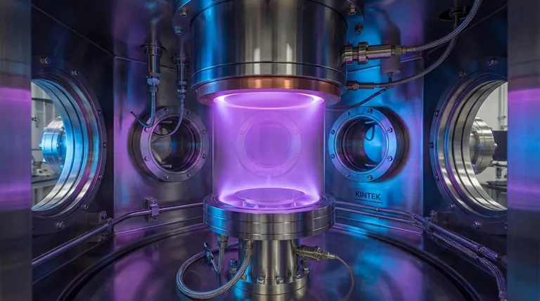
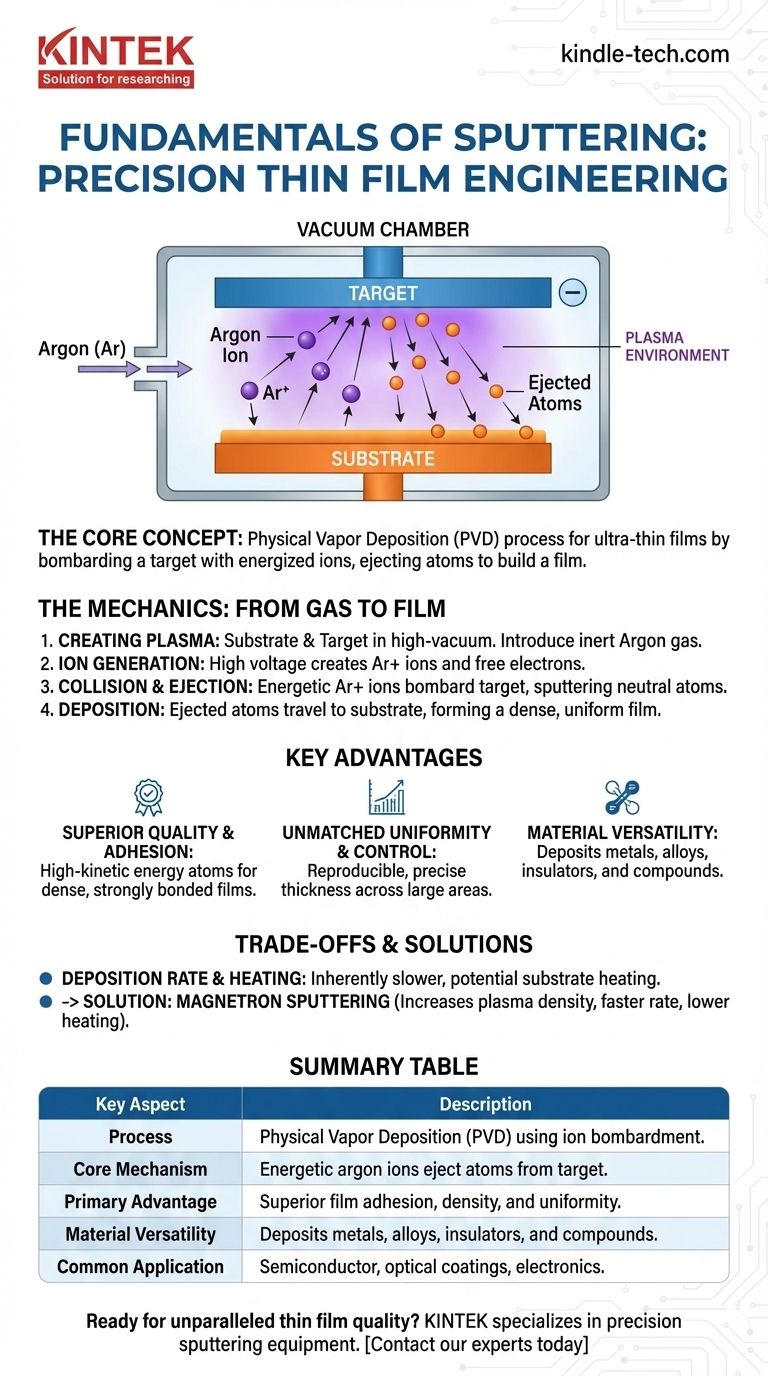
At its core, sputtering is a physical vapor deposition (PVD) process used to create ultra-thin films of material. It works by bombarding a solid source material, called a "target," with energized ions in a vacuum. These collisions act like a microscopic sandblaster, ejecting atoms from the target, which then travel and deposit onto a substrate, building a film one atom at a time.
Sputtering is not simply a method for coating a surface; it is a highly controlled engineering process for creating thin films with superior adhesion, density, and uniformity. Its value lies in the quality and precision of the resulting film, not the speed of deposition.
The Mechanics of Sputtering: From Gas to Film
To understand sputtering, it's best to break it down into a sequence of events that occur within a controlled vacuum chamber.
Creating the Plasma Environment
The process begins by placing the substrate and the target material into a high-vacuum chamber. The chamber is pumped down to remove air and other contaminants.
Once evacuated, a small, controlled amount of an inert gas, most commonly argon, is introduced into the chamber.
Ion Generation and Acceleration
A high negative voltage is applied to the target material. This strong electric field energizes free electrons in the chamber.
These high-energy electrons collide with the neutral argon atoms, knocking an electron off and creating positively charged argon ions (Ar+). This mixture of ions and electrons forms a low-temperature plasma.
Because the target is negatively charged and the argon ions are positively charged, the ions are aggressively accelerated toward the face of the target.
The Collision and Ejection Process
Upon impact, the high-energy argon ion transfers its kinetic energy and momentum to the atoms in the target. This is a purely physical, mechanical process.
If the energy transfer is sufficient, it "sputters" or ejects an atom from the target material. These ejected particles are typically neutral atoms, not ions.
Deposition on the Substrate
The ejected atoms travel in a relatively straight line from the target toward the substrate, which is usually positioned directly opposite it.
When these energetic atoms arrive at the substrate, they condense on its surface. Over time, millions of these arriving atoms build up to form a thin, dense, and highly uniform film.
Why Sputtering Excels: The Key Advantages
Sputtering is chosen over other deposition methods for several critical reasons related to film quality and material versatility.
Superior Film Quality and Adhesion
The sputtered atoms arrive at the substrate with significant kinetic energy. This energy helps them form a denser film and provides much stronger adhesion to the substrate compared to lower-energy processes like thermal evaporation.
Unmatched Uniformity and Control
The process is highly reproducible and can be precisely controlled by managing gas pressure, voltage, and deposition time. This results in excellent film thickness uniformity across large substrates, a critical requirement for semiconductors, optical filters, and precision electronics.
Versatility in Materials
Sputtering can deposit nearly any material, including pure metals, insulators, and semiconductors. Crucially, it excels at depositing alloys and compounds, as the ejection process generally preserves the chemical composition (stoichiometry) of the target.
Understanding the Trade-offs and Limitations
While powerful, sputtering is not without its challenges. Understanding these trade-offs is key to knowing when to use it.
The Challenge of Deposition Rate
Basic sputtering is an inherently slow process compared to techniques like thermal evaporation. The rate of film growth is a fundamental trade-off for achieving high film quality and control.
Substrate Heating Concerns
The constant energy bombardment from the plasma and depositing atoms can heat the substrate. In early systems, this limited the ability to coat heat-sensitive materials like plastics without causing damage.
The Magnetron Solution
Most modern sputtering systems use magnetron sputtering. By placing powerful magnets behind the target, electrons are trapped in a magnetic field close to the target's surface.
This trapping dramatically increases the probability of electrons colliding with and ionizing the argon gas. This creates a much denser plasma, which significantly increases the deposition rate and allows the system to run at lower pressures, reducing substrate heating.
When to Choose Sputtering
Sputtering is a specialized tool, and its use should be aligned with your project's most critical goals.
- If your primary focus is film quality and adhesion: Sputtering is an exceptional choice due to the high-energy deposition that creates dense, strongly bonded layers.
- If your primary focus is depositing complex alloys or compounds: Sputtering offers superior control, allowing you to maintain the composition of the source material or even create new compounds by adding reactive gases (e.g., nitrogen to form nitrides).
- If your primary focus is mass production speed at the lowest cost: You must evaluate if sputtering's slower deposition rate is acceptable for your needs, or if a faster process like thermal evaporation provides "good enough" quality.
Ultimately, sputtering is the definitive process for applications where the precision, purity, and integrity of the thin film cannot be compromised.
Summary Table:
| Key Aspect | Description |
|---|---|
| Process | Physical Vapor Deposition (PVD) using ion bombardment. |
| Core Mechanism | Energetic argon ions eject atoms from a target material. |
| Primary Advantage | Superior film adhesion, density, and uniformity. |
| Material Versatility | Deposits metals, alloys, insulators, and compounds. |
| Common Application | Semiconductor manufacturing, optical coatings, electronics. |
Ready to achieve unparalleled thin film quality in your lab? KINTEK specializes in precision sputtering equipment and consumables, providing the tools and expertise to create dense, uniform films with superior adhesion. Whether you're working on semiconductors, research, or advanced coatings, our solutions are engineered for performance and reliability. Contact our experts today to discuss how we can support your laboratory's specific needs!
Visual Guide
Related Products
- Spark Plasma Sintering Furnace SPS Furnace
- Vacuum Induction Melting Spinning System Arc Melting Furnace
- Chemical Vapor Deposition CVD Equipment System Chamber Slide PECVD Tube Furnace with Liquid Gasifier PECVD Machine
- Customer Made Versatile CVD Tube Furnace Chemical Vapor Deposition Chamber System Equipment
People Also Ask
- What is the mechanism of SPS process? A Deep Dive into Rapid, Low-Temperature Sintering
- Why are Spark Plasma Sintering (SPS) furnaces or hot presses utilized in the preparation of Li3PS4 solid electrolytes?
- What are the fundamentals of spark plasma sintering process? Unlock Rapid, High-Performance Material Consolidation
- What is SPS sintering method? A Guide to High-Speed, High-Performance Material Fabrication
- What is the theory of spark plasma sintering? A Guide to Rapid, Low-Temperature Densification


