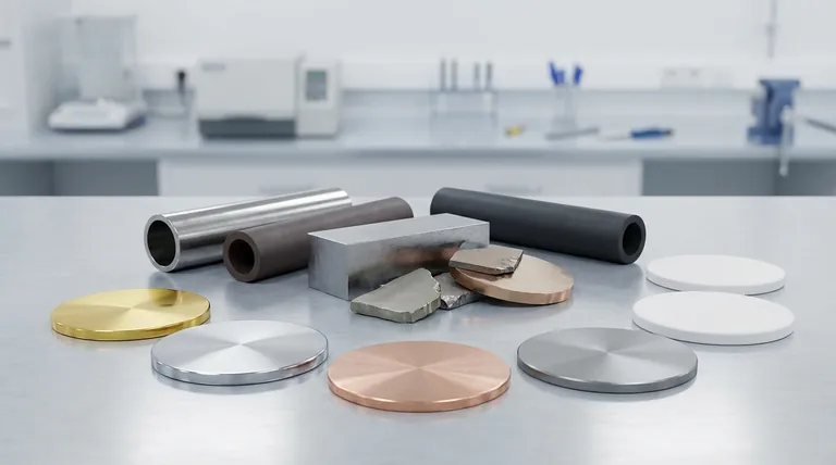
In short, sputtering can deposit a vast range of materials. The process is remarkably versatile, capable of creating thin films from pure metals like gold and silver, complex alloys like steel, and insulating ceramic compounds such as metal oxides and nitrides. The material you wish to deposit is fabricated into a physical "target" that is eroded during the process.
The versatility of sputtering is its greatest strength, but the fundamental choice of your target material dictates the entire setup. The core distinction is whether the material is electrically conductive or insulating, which determines the type of power supply and process required.
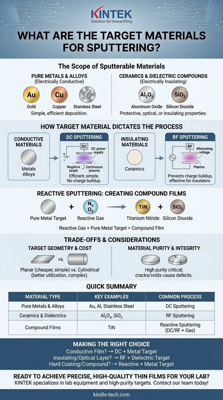
The Scope of Sputterable Materials
The sputtering process places very few restrictions on the types of materials that can be deposited. This flexibility is a primary reason for its widespread use in industries from semiconductor manufacturing to medical devices.
Pure Metals and Alloys
The most straightforward materials for sputtering are pure metals and their alloys. These materials are electrically conductive, which simplifies the sputtering process.
Common examples include:
- Precious metals: Gold (Au), Silver (Ag), Platinum (Pt)
- Industrial metals: Copper (Cu), Aluminum (Al), Titanium (Ti)
- Alloys: Stainless steel, Gold-Palladium (Au-Pd)
Ceramics and Dielectric Compounds
Sputtering is also highly effective for depositing ceramics and other dielectric (electrically insulating) materials.
These are often used for their protective, optical, or insulating properties. Examples include Aluminum Oxide (Al₂O₃), Silicon Dioxide (SiO₂), and Titanium Dioxide (TiO₂).
How Target Material Dictates the Sputtering Process
The choice of target material isn't just about the final film; it determines the physics of the sputtering process itself, primarily the power source needed to sustain the plasma.
Conductive Materials and DC Sputtering
For electrically conductive materials like metals and alloys, a Direct Current (DC) power supply is used.
DC sputtering is efficient and relatively simple. A negative voltage is applied to the target, which attracts positive ions from the plasma, causing the sputtering to occur. This process is continuous and stable for conductive targets.
Insulating Materials and RF Sputtering
For electrically insulating materials like ceramics, a DC power supply will not work. A positive charge would quickly build up on the target's surface, repelling the positive plasma ions and stopping the sputtering process.
The solution is to use a Radio Frequency (RF) power supply. The RF field rapidly alternates the voltage, preventing charge buildup and allowing both insulators and semiconductors to be sputtered effectively.
Creating Compounds with Reactive Sputtering
You can also create compound films like nitrides or oxides from a pure metal target through a process called reactive sputtering.
In this technique, a reactive gas like nitrogen (N₂) or oxygen (O₂) is introduced into the vacuum chamber along with the inert gas (like Argon). The sputtered metal atoms react with this gas on their way to the substrate, forming a compound film like Titanium Nitride (TiN) or Silicon Dioxide (SiO₂).
Understanding the Trade-offs and Considerations
Beyond the material's electrical properties, the physical characteristics of the target itself have practical and financial implications for the sputtering process.
Target Geometry and Cost
Sputtering targets come in various shapes, most commonly planar (flat) discs or cylindrical/ring-shaped tubes.
Planar targets are generally cheaper and easier to manufacture and replace. However, some system designs require cylindrical or ring-shaped targets, which offer better material utilization but are more expensive and complex.
Material Purity and Integrity
The quality of the target material is paramount. It must be of high purity to prevent contamination of the thin film.
Furthermore, the target must be physically robust and free of cracks or voids. These defects can cause inconsistent sputtering rates, arcing in the plasma, and particle generation, all of which compromise the quality of the final coating.
Making the Right Choice for Your Application
Selecting the right target and process depends entirely on the properties you need in your final thin film.
- If your primary focus is depositing a simple, conductive metallic film: A pure metal target using a straightforward DC sputtering process is the most efficient choice.
- If your primary focus is creating an insulating, ceramic, or optical layer: You must use an RF sputtering process with a target made of that specific dielectric material (e.g., an Al₂O₃ target).
- If your primary focus is creating a hard coating or compound film like a nitride: Reactive sputtering using a pure metal target and a reactive gas is often the most cost-effective and controllable method.
Ultimately, understanding the link between the target material and the sputtering method empowers you to achieve a precise and high-quality coating for nearly any application.
Summary Table:
| Material Type | Key Examples | Common Sputtering Process |
|---|---|---|
| Pure Metals & Alloys | Gold (Au), Aluminum (Al), Stainless Steel | DC Sputtering |
| Ceramics & Dielectrics | Aluminum Oxide (Al₂O₃), Silicon Dioxide (SiO₂) | RF Sputtering |
| Compound Films (via Reactive Sputtering) | Titanium Nitride (TiN) | Reactive Sputtering (DC/RF + Reactive Gas) |
Ready to achieve precise, high-quality thin films for your lab? The right sputtering target material is critical to your success. KINTEK specializes in lab equipment and consumables, offering expert guidance and high-purity targets for metals, alloys, and ceramics. Let our expertise help you select the optimal material and process for your specific application. Contact our team today to discuss your project needs!
Visual Guide
Related Products
- Laboratory CVD Boron Doped Diamond Materials
- Boron Nitride (BN) Ceramic Plate
- Reference Electrode Calomel Silver Chloride Mercury Sulfate for Laboratory Use
- Electron Beam Evaporation Coating Oxygen-Free Copper Crucible and Evaporation Boat
- Cylindrical Press Mold with Scale for Lab
People Also Ask
- What is the demand of CVD diamonds? Driven by Ethics, Purity, and Affordability
- What is the purpose of performing anodic polarization on BDD electrodes? Ensure Accurate & Reproducible Research Results
- How much cheaper are CVD diamonds? Save 20-30% on a Genuine Diamond
- Do CVD diamonds pass diamond tester? Yes, they are real diamonds.
- What are the applications of CVD diamonds? From Jewelry to High-Tech Tools


