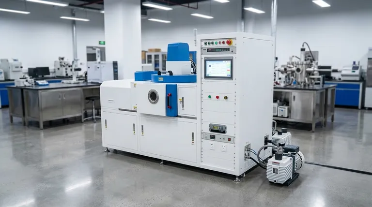
At its core, magnetron sputtering is a highly versatile manufacturing process used to deposit exceptionally thin, high-performance films of material onto a substrate. This physical vapor deposition (PVD) technique is a cornerstone technology in industries ranging from microelectronics and optics to automotive and medical devices. Its primary use is to fundamentally alter the surface properties of an object, granting it new capabilities like enhanced durability, specific optical qualities, or electrical conductivity.
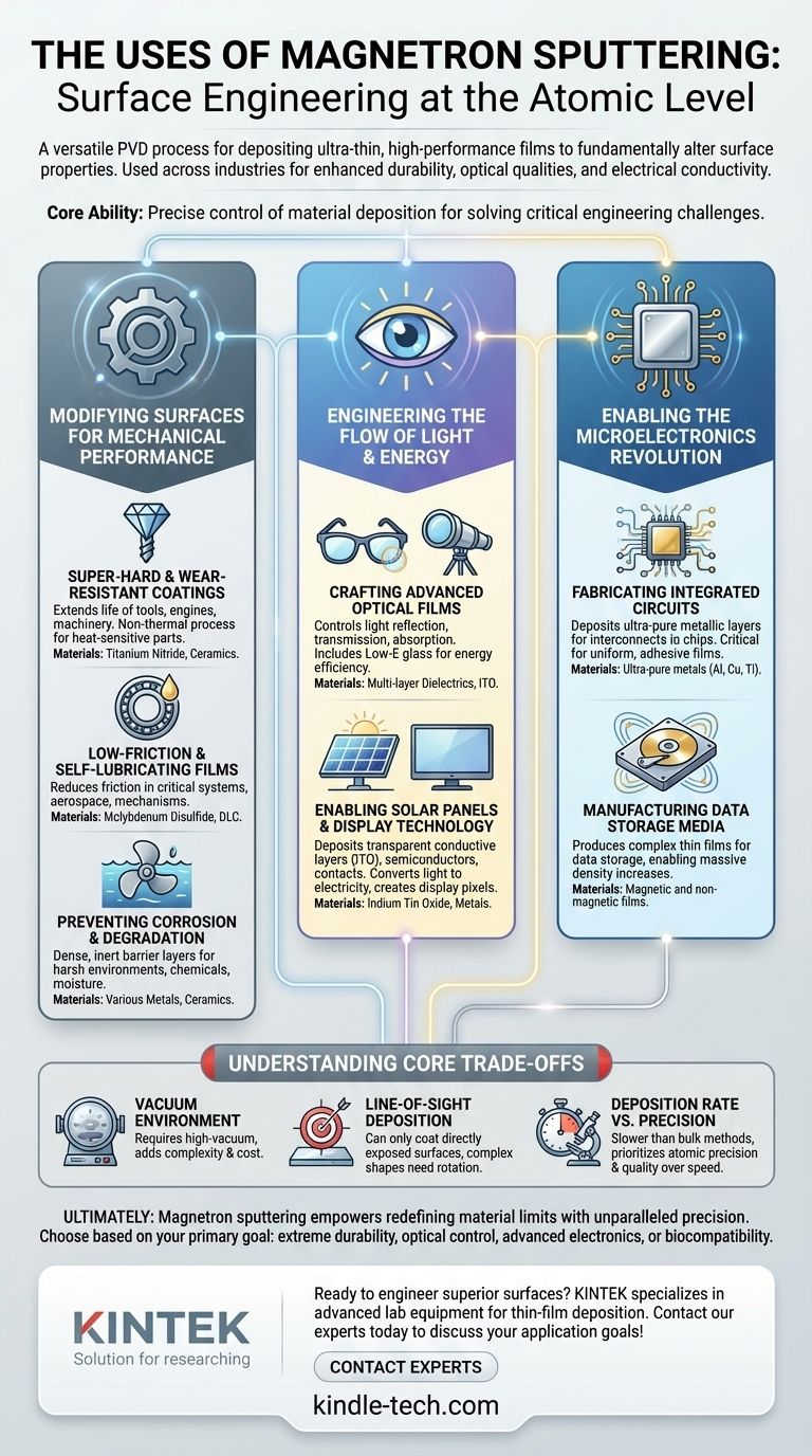
The true power of magnetron sputtering isn't in any single application, but in its fundamental ability to engineer material surfaces at the atomic level. By precisely controlling the deposition of thin films, we can solve critical engineering challenges across a vast spectrum of industries.
Modifying Surfaces for Mechanical Performance
Magnetron sputtering is the go-to method for creating surfaces that can withstand extreme physical stress. This is achieved by depositing films that are harder, slicker, or more resilient than the underlying material.
Creating Super-Hard and Wear-Resistant Coatings
For tools and components that experience intense friction and wear, sputtered coatings provide a crucial layer of defense. These films, often made of ceramic materials like titanium nitride, dramatically extend the life of cutting tools, engine components, and industrial machinery.
This is a non-thermal process, meaning it can coat heat-sensitive parts without altering their fundamental structure or temper.
Designing Low-Friction and Self-Lubricating Films
In applications where reducing friction is critical, sputtering can apply solid lubricants like molybdenum disulfide or diamond-like carbon (DLC). These films are essential for high-performance bearings, aerospace mechanisms, and other systems where traditional liquid lubricants would fail.
Preventing Corrosion and Degradation
Sputtering is also used to deposit dense, inert barrier layers that protect a substrate from its environment. These corrosion-resistant coatings are vital for components exposed to harsh chemicals, moisture, or salt, from gas turbine blades in jet engines to fixtures in marine environments.
Engineering the Flow of Light and Energy
Many modern technologies depend on the ability to precisely control how light and other forms of energy interact with a surface. Sputtering provides the atomic-scale precision needed to build these complex optical and electrical structures.
Crafting Advanced Optical Films
From the anti-reflective coating on your eyeglasses to the mirror on a space telescope, sputtered films are essential. By depositing multiple, ultra-thin layers of materials with different refractive indices, engineers can create coatings that selectively reflect, transmit, or absorb specific wavelengths of light.
A prominent example is Low-emissivity (Low-E) glass used in modern architecture, which has a sputtered coating that reflects infrared heat while allowing visible light to pass through, dramatically improving energy efficiency.
Enabling Solar Panels and Display Technology
The functionality of solar cells and flat-panel displays relies on sputtered thin films. Sputtering is used to deposit the transparent conductive layers (like Indium Tin Oxide, or ITO), semiconductor materials, and metallic contacts that are required to convert light into electricity or to create the pixels in an LCD or OLED screen.
Enabling the Microelectronics Revolution
The incredible density and performance of modern electronics would not be possible without magnetron sputtering. The process is fundamental to the fabrication of integrated circuits and data storage devices.
Fabricating Integrated Circuits
In semiconductor manufacturing, sputtering is used to deposit the ultra-pure metallic layers that form the microscopic "wiring" connecting the billions of transistors on a single chip. Its ability to create uniform, highly adhesive films is critical for device reliability and performance.
Manufacturing Data Storage Media
Magnetron sputtering was an early and essential technology for producing computer hard disks. The process is used to deposit the complex stack of magnetic and non-magnetic thin films that store data, enabling the massive increases in storage density we see today.
Understanding the Core Trade-offs
While incredibly powerful, magnetron sputtering is not a universal solution. Understanding its limitations is key to using it effectively.
Requirement for a Vacuum Environment
Sputtering must be performed inside a high-vacuum chamber to prevent the deposited atoms from reacting with air. This makes the equipment more complex and expensive than atmospheric processes like painting or electroplating.
"Line-of-Sight" Deposition
In its basic form, sputtering is a "line-of-sight" technique, meaning it can only coat surfaces directly exposed to the sputtering target. Coating complex, three-dimensional shapes uniformly requires sophisticated part-rotation systems, which adds to process complexity.
Deposition Rate vs. Precision
While faster than some other PVD methods, sputtering can be a relatively slow process compared to bulk coating techniques. The trade-off is one of speed versus control; sputtering prioritizes atomic-level precision and film quality over rapid material buildup.
Making the Right Choice for Your Goal
The decision to use magnetron sputtering depends entirely on the problem you need to solve.
- If your primary focus is extreme durability: Sputtering is a leading choice for creating hard, wear-resistant, and low-friction coatings on critical components.
- If your primary focus is optical control: It is the industry standard for high-precision coatings on lenses, windows, and filters.
- If your primary focus is advanced electronics: Sputtering is an indispensable and non-negotiable process for fabricating modern semiconductors and data storage media.
- If your primary focus is biocompatibility or aesthetics: The technology excels at applying inert coatings to medical implants and creating durable, decorative finishes for consumer goods.
Ultimately, magnetron sputtering empowers engineers and scientists to redefine the limits of materials by controlling their surfaces with unparalleled precision.
Summary Table:
| Application Area | Key Uses | Common Materials |
|---|---|---|
| Mechanical Performance | Wear-resistant coatings, low-friction films, corrosion barriers | Titanium Nitride, DLC, Molybdenum Disulfide |
| Optical & Energy | Anti-reflective coatings, Low-E glass, solar cells, displays | Indium Tin Oxide (ITO), multi-layer dielectrics |
| Microelectronics | Semiconductor interconnects, data storage media | Ultra-pure metals (Al, Cu, Ti) |
| Medical & Decorative | Biocompatible implants, durable aesthetic finishes | Gold, Titanium, Ceramics |
Ready to engineer superior surfaces with magnetron sputtering? KINTEK specializes in advanced lab equipment and consumables for thin-film deposition, serving R&D and production labs across industries. Whether you're developing wear-resistant components, optical coatings, or next-generation electronics, our solutions deliver the precision and reliability you need. Contact our experts today to discuss how we can support your specific application goals!
Visual Guide
Related Products
- Microwave Plasma Chemical Vapor Deposition MPCVD Machine System Reactor for Lab and Diamond Growth
- Chemical Vapor Deposition CVD Equipment System Chamber Slide PECVD Tube Furnace with Liquid Gasifier PECVD Machine
- Molybdenum Tungsten Tantalum Special Shape Evaporation Boat
- Inclined Rotary Plasma Enhanced Chemical Vapor Deposition PECVD Equipment Tube Furnace Machine
- Inclined Rotary Plasma Enhanced Chemical Vapor Deposition PECVD Equipment Tube Furnace Machine
People Also Ask
- How do vacuum pumps and valves collaborate in MPCVD? Achieve Precise Pressure Control for Superior CNT Synthesis
- How is a diamond formed from CVD? The Science of Growing Diamonds Atom by Atom
- What are the advantages of a Microwave Plasma CVD reactor for MCD/NCD coatings? Precision Multilayer Diamond Engineering
- What pressure is needed for chemical vapor deposition of diamonds? Master the Low-Pressure 'Sweet Spot'
- How are CVD diamonds created? Discover the Science of Lab-Grown Diamond Precision