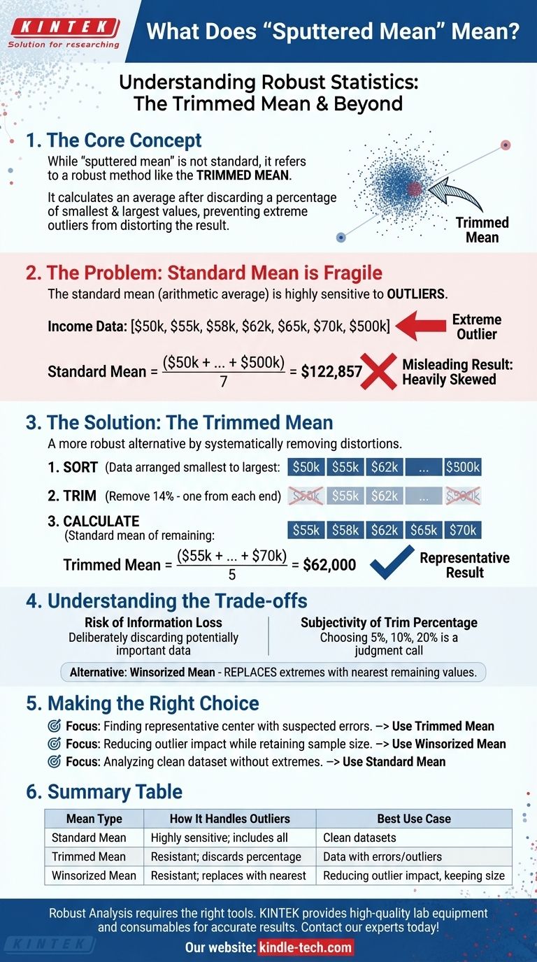
While "sputtered mean" is not a standard statistical term, it almost certainly refers to a robust method of calculating an average that is resistant to outliers, most likely the trimmed mean. A trimmed mean, also known as a truncated mean, calculates the average of a dataset after discarding a certain percentage of the smallest and largest values. This prevents extreme, and possibly erroneous, data points from distorting the final result.
The core idea behind a trimmed mean is to get a more reliable and representative average from "messy" data. By intentionally ignoring the most extreme values on both ends, you calculate a central value that better reflects the bulk of your data points.

The Problem: Why a Standard Mean is Fragile
The standard average, or arithmetic mean, is a fundamental concept. However, it has one significant weakness: it is highly sensitive to outliers.
The Influence of Extreme Values
An outlier is a data point that is abnormally distant from other values in a dataset. A single extreme value can dramatically pull the standard mean in its direction.
For example, consider the reported annual incomes for a small team of seven people: [$50k, $55k, $58k, $62k, $65k, $70k, $500k].
The standard mean is $122,857. This number doesn't accurately represent any single person on the team and is heavily skewed by the one high earner.
The Solution: The Trimmed Mean
The trimmed mean offers a more robust alternative by systematically removing these distortions.
How a Trimmed Mean Works
The process is straightforward:
- Sort the data from smallest to largest.
- Trim a small, predetermined percentage of values from both the top and bottom of the sorted list.
- Calculate the standard mean of the remaining data.
The Previous Example, Revisited
Using our income data and applying a 14% trim (which corresponds to removing one value from each end of our seven-point list), we first remove $50k and $500k.
The remaining values are [$55k, $58k, $62k, $65k, $70k].
The new trimmed mean is $62,000. This figure is a much more realistic and representative measure of the team's typical income.
Understanding the Trade-offs
Using a trimmed mean is a powerful technique, but it isn't a universal solution. It involves making a judgment call that comes with trade-offs.
The Risk of Information Loss
When you trim data, you are deliberately discarding information. If the extreme values you remove are not errors but are in fact legitimate and important data points, you risk biasing your understanding of the dataset.
The Subjectivity of the Trim Percentage
Choosing how much to trim (e.g., 5% vs. 10% vs. 20%) is a subjective decision. There is no single "correct" percentage, and different choices can lead to different results. This decision should be based on your understanding of the data and why it might contain outliers.
When to Use a Related Method: The Winsorized Mean
Another robust statistic is the Winsorized mean. Instead of deleting the extreme values, it replaces them with the nearest remaining values. This allows you to retain the original number of data points while still reducing the impact of outliers.
Making the Right Choice for Your Data
To decide which type of mean to use, you must first clarify your analytical goal.
- If your primary focus is finding a representative center for data with known or suspected errors: The trimmed mean is an excellent choice for completely removing the influence of extreme outliers.
- If your primary focus is reducing outlier impact while retaining your original sample size: The Winsorized mean is a more suitable option.
- If your primary focus is analyzing a clean, well-behaved dataset without extreme outliers: The standard arithmetic mean remains the most direct and statistically efficient measure.
Ultimately, choosing the right method is about ensuring the final number accurately reflects the true story your data is telling.
Summary Table:
| Mean Type | How It Handles Outliers | Best Use Case |
|---|---|---|
| Standard Mean | Highly sensitive; includes all data points. | Clean datasets without extreme values. |
| Trimmed Mean | Resistant; discards a percentage of extreme values. | Data with known/suspected errors or outliers. |
| Winsorized Mean | Resistant; replaces extreme values with nearest values. | Reducing outlier impact while keeping sample size. |
Ready to ensure your data analysis is robust and reliable? The right statistical tools are just as important as the right lab equipment. At KINTEK, we specialize in providing the high-quality lab equipment and consumables your research depends on. Let us help you build a foundation for accurate results.
Contact our experts today to discuss your laboratory needs!
Visual Guide