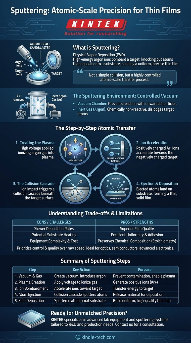
At its core, sputtering is a physical vapor deposition (PVD) process that functions like an atomic-scale sandblaster. Inside a high vacuum, energized ions of an inert gas (typically argon) are accelerated to bombard a source material, known as the target. This high-energy collision physically knocks out, or "sputters," atoms from the target, which then travel and deposit onto a substrate, building up an exceptionally uniform and precise thin film.
Sputtering is best understood not as a simple collision, but as a highly controlled atomic-scale transfer process. By using energized gas ions to physically eject atoms from a source material, it enables the creation of ultra-thin films with precisely engineered properties on a separate surface.
The Sputtering Environment: A Controlled Vacuum
To understand the sputtering process, we must first understand the highly controlled environment where it takes place. This isn't a simple chemical reaction; it's a physical process that requires specific conditions to succeed.
The Role of the Vacuum Chamber
The entire sputtering process occurs within a vacuum chamber. Air is pumped out to remove oxygen, water vapor, and other atmospheric gases.
This vacuum is critical because it prevents the sputtered atoms from reacting with or being scattered by unwanted particles on their way from the target to the substrate.
Introducing the Inert Gas
Once a vacuum is established, a small, controlled amount of a high-purity inert gas, most commonly argon (Ar), is introduced.
Argon is used because it is chemically non-reactive and has a sufficient atomic mass to effectively dislodge atoms from the target material upon impact.
The Step-by-Step Atomic Transfer
With the stage set, the core sputtering mechanism can begin. This is a sequence of events that transforms a solid target material into a thin film on a substrate.
Step 1: Creating the Plasma
A high voltage is applied across the chamber, with the target material acting as the cathode (negative charge).
This electrical energy ionizes the argon gas atoms, stripping them of an electron and creating a mixture of positively charged argon ions (Ar+) and free electrons. This energized, ionized gas state is known as a plasma.
Step 2: Ion Acceleration and Bombardment
The positively charged argon ions are now strongly attracted and accelerated towards the negatively charged target material.
They gain significant kinetic energy as they travel, ultimately slamming into the target's surface at high velocity.
Step 3: The Collision Cascade
A single ion impact does more than just hit one atom. It transfers its momentum, setting off a chain reaction or "collision cascade" beneath the target's surface.
Atoms within the target material collide with their neighbors, transferring energy throughout the atomic lattice, much like a break in a game of pool.
Step 4: Ejection and Deposition
When this collision cascade reaches an atom on the target's surface with enough energy to overcome its atomic bonding forces, that atom is ejected, or sputtered, from the target.
These freed atoms travel through the vacuum chamber and land on the substrate, where they cool, condense, and gradually build up to form a thin, solid film.
Understanding the Trade-offs and Limitations
While powerful, sputtering is not a universal solution. Its effectiveness is defined by a distinct set of operational trade-offs that make it ideal for some applications and less suitable for others.
Slower Deposition Rates
Compared to other PVD methods like thermal evaporation, sputtering is generally a slower process. The mechanical nature of ejecting atoms one by one is less rapid than boiling a material.
This makes it less economical for depositing very thick films or for applications where high throughput is the primary concern.
Potential for Substrate Heating
The significant energy involved in the ion bombardment and film condensation can lead to heating of the substrate.
This can be a challenge when coating heat-sensitive materials, such as certain plastics or biological samples, and may require active cooling systems.
Equipment Complexity and Cost
Sputtering systems require a high-vacuum environment, sophisticated power supplies, and often magnetic fields (in magnetron sputtering) to operate efficiently.
This makes the initial equipment investment and operational complexity higher than for some alternative coating methods.
Making the Right Choice for Your Goal
The decision to use sputtering is fundamentally about prioritizing control and film quality over raw deposition speed.
- If your primary focus is precision and film quality: Sputtering offers superior control over film density, uniformity, adhesion, and morphology, making it ideal for optics, semiconductors, and advanced electronics.
- If your primary focus is deposition speed for simple coatings: Other methods like thermal evaporation might be more time- and cost-efficient for applications like basic metallization.
- If your primary focus is coating complex alloys or compounds: Sputtering excels because it generally preserves the chemical composition (stoichiometry) of the target material in the resulting film.
Ultimately, understanding the sputtering mechanism empowers you to select a deposition method that perfectly matches the required precision and material characteristics of your application.
Summary Table:
| Sputtering Step | Key Action | Purpose |
|---|---|---|
| 1. Vacuum & Gas | Create vacuum, introduce argon gas | Prevent contamination, enable plasma |
| 2. Plasma Creation | Apply voltage to ionize argon gas | Generate positive ions (Ar+) |
| 3. Ion Bombardment | Accelerate ions toward target (cathode) | Transfer energy to target atoms |
| 4. Atom Ejection | Collision cascade sputters target atoms | Release material for deposition |
| 5. Film Deposition | Sputtered atoms travel and coat substrate | Build uniform, high-quality thin film |
Ready to Achieve Unmatched Precision in Your Thin Film Applications?
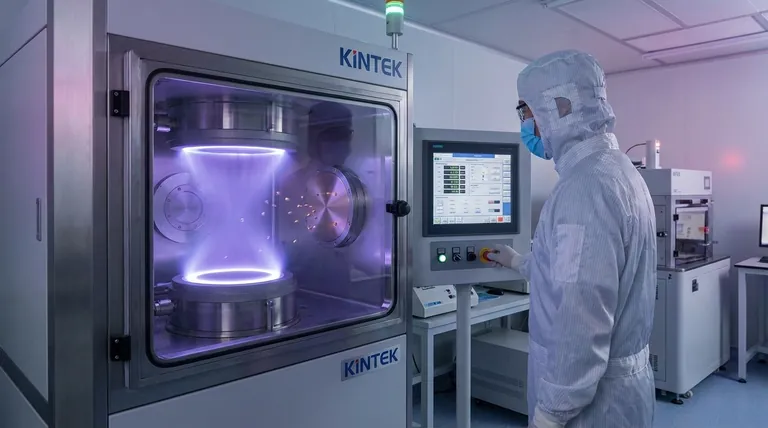
Sputtering is the gold standard for creating high-performance coatings, but achieving optimal results requires the right equipment and expertise. KINTEK specializes in advanced lab equipment and consumables, providing robust sputtering systems and targets tailored to the exacting needs of R&D and production laboratories.
Whether you are developing next-generation semiconductors, precision optics, or advanced sensors, our solutions deliver the superior film uniformity, adhesion, and stoichiometric control critical for your success.
Let's discuss how a KINTEK sputtering system can elevate your research and manufacturing. Contact our experts today for a personalized consultation.
Visual Guide
Related Products
- Spark Plasma Sintering Furnace SPS Furnace
- Vacuum Induction Melting Spinning System Arc Melting Furnace
- Chemical Vapor Deposition CVD Equipment System Chamber Slide PECVD Tube Furnace with Liquid Gasifier PECVD Machine
- Customer Made Versatile CVD Tube Furnace Chemical Vapor Deposition Chamber System Equipment
People Also Ask
- What are the advantages of CAMI/SPS for W-Cu composite preparation? Reduce cycles from hours to seconds.
- What is the process fundamentals of spark plasma sintering? Achieve Rapid, High-Density Material Consolidation
- What are the fundamentals of spark plasma sintering process? Unlock Rapid, High-Performance Material Consolidation
- What is SPS sintering method? A Guide to High-Speed, High-Performance Material Fabrication
- What is the theory of spark plasma sintering? A Guide to Rapid, Low-Temperature Densification


