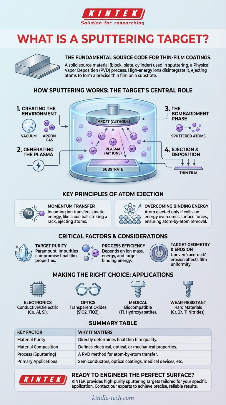
In the world of advanced materials science and manufacturing, a sputtering target is the solid source material used in a high-vacuum coating process known as sputtering. It is a block, plate, or cylinder of a specific substance that is intentionally disintegrated by high-energy ions. This process ejects atoms from the target, creating a vapor that deposits as a precisely controlled thin film onto a separate object, the substrate.
A sputtering target is not merely a piece of raw material; it is the fundamental source code for a thin-film coating. Its composition, purity, and physical form directly dictate the properties of the final engineered surface, from the electrical pathways in a microchip to the anti-reflective coating on a pair of glasses.
How Sputtering Works: The Target's Central Role
To understand what a sputtering target is, one must first understand the process it enables. Sputtering is a Physical Vapor Deposition (PVD) method, meaning it uses physical mechanics, not chemical reactions, to transfer material.
Creating the Environment
The entire process occurs inside a sealed vacuum chamber. This chamber contains the sputtering target (the source material) and the substrate (the object to be coated). The chamber is filled with a small, controlled amount of an inert gas, most commonly Argon.
Generating the Plasma
A powerful voltage is applied within the chamber, establishing the target as the cathode (negative charge). This electrical potential energizes the Argon gas, stripping electrons from the Argon atoms and creating a glowing, ionized gas known as a plasma. These newly formed, positively charged Argon ions (Ar+) are now free within the chamber.
The Bombardment Phase
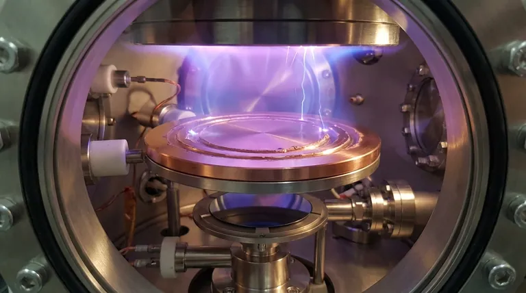
The core of the process is an electrical attraction. The positively charged Argon ions are forcefully accelerated by the electric field, causing them to slam into the negatively charged surface of the sputtering target at extremely high velocity.
Ejection and Deposition
This high-energy ionic bombardment acts like a microscopic sandblaster. The impact of each Argon ion transfers significant kinetic energy to the target material, setting off a "collision cascade" within its atomic structure. When this chain reaction of collisions reaches the surface, it ejects individual atoms or molecules from the target.
These sputtered particles travel through the vacuum chamber and land on the substrate, condensing to form a thin, uniform film.
Key Principles of Target Atom Ejection
The sputtering of a target is governed by fundamental physics, not by melting or evaporation. Understanding these principles shows why the process is so highly controllable.
Momentum Transfer
At its heart, sputtering is a process of momentum transfer. An incoming gas ion is like a cue ball striking a rack of billiard balls (the target atoms). The energy and angle of the impact directly influence how many atoms are ejected and with what energy.
Overcoming Surface Binding Energy
An atom is only ejected from the target if the collision cascade provides it with enough energy to overcome the surface binding energy—the force that holds the atom to the rest of the material. This is why sputtering is a controlled, atom-by-atom removal process rather than a chaotic melting event.
Critical Factors and Considerations
The success and quality of a sputtering process are directly tied to the target and the conditions surrounding it. Ignoring these factors leads to flawed or inconsistent coatings.
Target Material Purity
The purity of the sputtering target is paramount. Any impurity within the target material will be sputtered along with the desired atoms and will become an impurity in the final thin film, potentially compromising its electrical, optical, or mechanical properties.
Process Efficiency
The rate at which atoms are ejected from the target—the sputtering yield—is not the same for all materials. It depends on the mass of the inert gas ion (heavier ions like Xenon are more efficient than Argon), the energy of the ions, and the binding energy of the target material itself. Some materials are simply "harder" to sputter than others.
Target Geometry and Erosion
As the process continues, the target material is consumed, or "eroded." This erosion typically happens unevenly, creating a "racetrack" pattern on the target's surface. Managing this erosion is critical for ensuring the deposited film remains uniform over time.
Making the Right Choice for Your Goal
The selection of a sputtering target is dictated entirely by the desired properties and function of the final thin-film coating.
- If your primary focus is electronics and semiconductors: You will use targets of highly pure conductive, resistive, or dielectric materials like copper, tantalum, aluminum, or silicon to create circuits and insulating layers.
- If your primary focus is optics and glass coatings: You will select targets made of transparent oxides like silicon dioxide (SiO2) or titanium dioxide (TiO2) to create anti-reflective or reflective layers.
- If your primary focus is medical devices and implants: You will use biocompatible targets like pure titanium or hydroxyapatite to create durable, non-reactive coatings that are safe for the human body.
- If your primary focus is wear-resistant or decorative finishes: You will use targets of hard materials like chromium, zirconium, or titanium to produce nitrides and carbonitrides for durable and aesthetically pleasing surfaces on tools, watches, and fixtures.
Ultimately, the sputtering target is the precise blueprint, atom by atom, for the high-performance surface you intend to create.
Summary Table:
| Key Factor | Why It Matters |
|---|---|
| Material Purity | Directly determines the quality and performance of the final thin film. |
| Material Composition | Defines the electrical, optical, or mechanical properties of the coating. |
| Process (Sputtering) | A Physical Vapor Deposition (PVD) method for atom-by-atom transfer. |
| Primary Applications | Semiconductors, optical coatings, medical devices, and durable finishes. |
Ready to engineer the perfect surface?
The right sputtering target is the foundation of your coating's success. KINTEK specializes in providing high-purity lab equipment and consumables, including sputtering targets tailored for your specific application—whether in semiconductor fabrication, optics, medical technology, or industrial coatings.
Let us help you achieve precise, reliable results. Contact our experts today to discuss your project requirements and discover how our solutions can enhance your manufacturing process.
Visual Guide
Related Products
- Reference Electrode Calomel Silver Chloride Mercury Sulfate for Laboratory Use
- Multifunctional Electrolytic Electrochemical Cell Water Bath Single Layer Double Layer
- Molybdenum Tungsten Tantalum Special Shape Evaporation Boat
- Hemispherical Bottom Tungsten Molybdenum Evaporation Boat
- Cylindrical Press Mold with Scale for Lab
People Also Ask
- What is the purpose of the reference electrode? Achieve Stable & Accurate Electrochemical Measurements
- What is the recommended maintenance for the filling solution of a reference electrode? A Guide to Stable & Accurate Readings
- What is the reference electrode in potentiometry? The Key to Stable & Accurate Measurements
- How does the selection of reference electrodes correlate with electrolyte pH in HER testing? Ensure Precise Potential
- Which electrode is used as a reference electrode for measuring half-cell potentials? Understanding the Universal Standard


