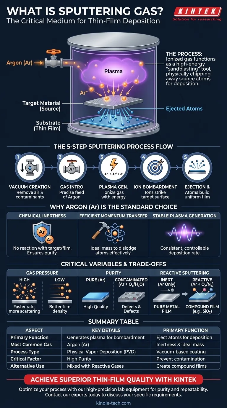
In thin-film deposition, sputtering gas is the critical medium used to generate the energetic particles that create the coating. It is typically a high-purity inert gas, like Argon, which is introduced into a vacuum chamber and then ionized to form a plasma. These ions are accelerated to bombard a source material (the "target"), physically knocking atoms from it that then deposit onto a substrate to form a uniform thin film.
The sputtering gas is not part of the final coating; it functions as a high-energy "sandblasting" tool. By ionizing this gas to create a plasma, the sputtering process generates a stream of ions that physically chip away at a source material, atom by atom, to deposit a pristine thin film.

The Role of Gas in the Sputtering Process
Sputtering is a form of Physical Vapor Deposition (PVD), a process that happens entirely within a vacuum. The gas is the key facilitator that transfers energy from a power source to the target material.
Step 1: Creating a Vacuum
Before the gas is introduced, the sputtering chamber is pumped down to a very low pressure. This removes air and other contaminants, such as water vapor, which could otherwise react with the coating material and compromise the purity and properties of the final film.
Step 2: Introducing the Sputtering Gas
Once the required vacuum level is achieved, a small, precisely controlled amount of sputtering gas is fed into the chamber. Argon (Ar) is the most common choice for this role.
Step 3: Generating a Plasma
A strong electric or electromagnetic field is applied within the chamber. This high energy strips electrons from the gas atoms, creating a mixture of positively charged ions (e.g., Ar+) and free electrons. This energized, ionized gas is known as a plasma.
Step 4: Ion Bombardment
The target material is given a negative electrical charge, which strongly attracts the positively charged gas ions from the plasma. These ions accelerate toward the target, striking its surface with significant kinetic energy.
Step 5: Ejection and Deposition
The impact of each ion transfers momentum to the target's atoms, knocking them loose from the surface. These ejected atoms travel in a straight line through the vacuum chamber until they strike the substrate, gradually building up to form a dense, uniform thin film.
Why Argon is the Standard Choice
While other gases can be used, Argon is the industry standard for most sputtering applications for several key reasons.
Chemical Inertness
As a noble gas, Argon is chemically inert. It will not react with the target material, the substrate, or the chamber components. This ensures the deposited film is a pure representation of the source material.
Efficient Momentum Transfer
Argon's atomic mass is ideal for efficiently transferring momentum to most common target materials. It is heavy enough to dislodge atoms effectively without being so heavy that it causes excessive damage or implants itself into the target.
Stable Plasma Generation
Argon ionizes readily and sustains a stable, controllable plasma under typical sputtering conditions. This allows for a consistent and repeatable deposition rate, which is critical for manufacturing.
Understanding the Trade-offs
The choice and handling of the sputtering gas directly influence the final film's quality. Understanding the variables is crucial for process control.
The Impact of Gas Pressure
The pressure of the sputtering gas inside the chamber is a critical parameter. Higher pressure can increase the number of ions and thus the deposition rate, but it can also cause the ejected target atoms to collide with gas atoms, scattering them and potentially reducing film density.
The Critical Need for Purity
The sputtering gas must be exceptionally pure and dry. Any contaminants, like oxygen or water, can be incorporated into the growing film, leading to unwanted chemical compositions and defects that degrade its electrical, optical, or mechanical properties.
Reactive vs. Inert Sputtering
While Argon is used for depositing pure materials, sometimes a reactive gas like oxygen or nitrogen is intentionally mixed with it. This process, called reactive sputtering, is used to form compound films. For example, sputtering a silicon target in an oxygen-argon mixture will deposit a silicon dioxide (SiO₂) film.
Making the Right Choice for Your Goal
The gas you choose is dictated entirely by the type of film you intend to create.
- If your primary focus is depositing a pure metal or alloy: Your default choice should be a high-purity inert gas like Argon to prevent any chemical reactions during deposition.
- If your primary focus is creating a compound film (like an oxide or nitride): You will use a precisely controlled mixture of an inert gas (Argon) and a reactive gas (e.g., Oxygen or Nitrogen).
- If your primary focus is optimizing film quality and process control: You must prioritize the purity of the sputtering gas and the integrity of the vacuum to avoid any form of contamination.
Ultimately, the sputtering gas is the engine of the deposition process; its careful selection and management are fundamental to achieving a high-quality, functional thin film.
Summary Table:
| Aspect | Key Details |
|---|---|
| Primary Function | Generates plasma to bombard a target and eject atoms for deposition. |
| Most Common Gas | Argon (Ar), chosen for its inertness and ideal atomic mass. |
| Process Type | Physical Vapor Deposition (PVD). |
| Critical Factor | High purity is essential to prevent film contamination. |
| Alternative Use | Mixed with reactive gases (e.g., O₂, N₂) to create compound films. |
Achieve Superior Thin-Film Quality with KINTEK
Your choice of sputtering gas and process parameters is critical to the performance of your coatings. Whether you are depositing pure metals, alloys, or complex compounds, the right lab equipment ensures precision, purity, and repeatability.
KINTEK specializes in high-quality lab equipment and consumables for all your thin-film deposition needs. Our expertise can help you optimize your sputtering process for unparalleled results.
Contact our experts today to discuss how we can support your laboratory's specific requirements and drive your research or production forward.
Visual Guide
Related Products
- Electrolytic Electrochemical Cell Gas Diffusion Liquid Flow Reaction Cell
- Spark Plasma Sintering Furnace SPS Furnace
People Also Ask
- Why are electrolytic cells essential in titanium production? Powering Circular Efficiency and Cost Savings
- How does the design of an electrochemical electrolytic cell influence the coating uniformity? Optimize Your Catalysts
- What is the function of the electrolytic cell in the Cu-Cl cycle? Optimize Hydrogen Production & Energy Efficiency
- How does the design of an electrolytic cell affect the production yield of ferrate(VI)? Optimize Efficiency & Purity
- What is galvanic cell or electrolytic cell? Unlock the Secrets of Electrochemical Power