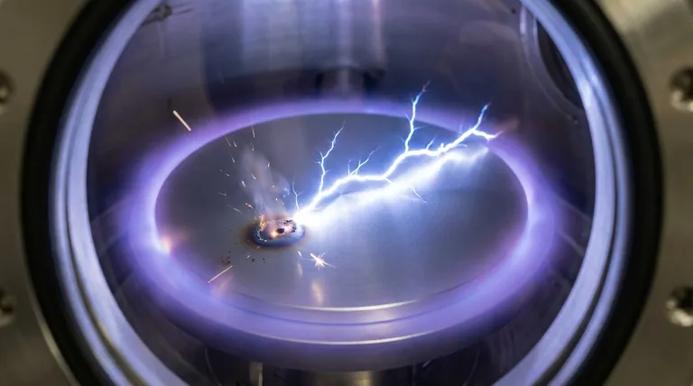
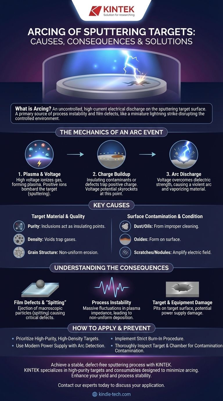
In the context of thin-film deposition, arcing is an uncontrolled, high-current electrical discharge that occurs on the surface of a sputtering target. This event is a primary source of process instability and film defects, functioning like a miniature lightning strike that disrupts the precisely controlled environment required for high-quality manufacturing.
Arcing is not a random failure but a symptom of an underlying issue, most commonly the buildup of electrical charge on insulating contaminants or defects on the target's surface. Understanding and controlling both the target's material quality and the process environment is the definitive way to prevent it.
The Mechanics of an Arc Event
To understand arcing, one must first understand the basic sputtering environment. A high voltage is applied to the target in a vacuum chamber filled with an inert gas, like argon, creating a plasma.
The Role of Plasma and Voltage
The high voltage causes the gas to ionize, forming a plasma of positive ions and free electrons. These positive ions are accelerated by the electric field and bombard the negatively charged target. This bombardment is the "sputtering" that ejects target material, which then deposits as a thin film on your substrate.
The Point of Failure: Charge Buildup
An ideal sputtering target is perfectly conductive, allowing the positive charge delivered by the incoming ions to dissipate instantly. An arc occurs when a localized spot on the target is unable to do this.
These spots are typically microscopic insulating layers, such as oxides, nitrides, or even dust particles. As positive ions bombard this insulating spot, the charge accumulates because it has nowhere to go. The voltage potential at this tiny point skyrockets relative to the surrounding target surface.
The "Lightning Strike" Discharge
When the accumulated voltage becomes high enough, it overcomes the dielectric strength of the insulating layer. The result is a sudden, violent discharge of current—an arc—that vaporizes a small amount of the target material and the contaminant.
Key Causes of Sputtering Target Arcing
Arcing is almost always a sign that something is wrong with the target material or the process environment. Identifying the root cause is critical for mitigation.
Target Material and Quality
The quality of the sputtering target itself is the most common factor. The initial reference to high-purity and high-density targets is relevant here because these attributes directly combat arcing.
- Purity: Foreign material inclusions within the target can become exposed during sputtering, acting as insulating points for charge buildup.
- Density: Low-density targets contain microscopic voids. These voids can trap process gases or become sources of internal arcing, which can destabilize the target surface.
- Grain Structure: Non-uniform grains can lead to uneven erosion rates, which may expose or create surface features that are more prone to arcing.
Surface Contamination and Condition
Even a perfect target can arc if its surface is compromised. Contaminants introduced into the vacuum chamber can land on the target and initiate an arc.
Common sources include dust from improper chamber cleaning, residual oils, or oxides that form on the target's surface before the process begins. Scratches or nodules on the surface can also create geometric points where the electric field is amplified, promoting discharge.
Understanding the Consequences
Arcing is more than a momentary flash; it has tangible, negative impacts on your process and your product. These consequences highlight why preventing arcing is a primary goal in any sputtering operation.
Film Defects and "Spitting"
The most damaging consequence of an arc is the ejection of macroscopic particles, or "droplets," of target material. This is often called spitting. These particles embed themselves in the growing thin film, creating critical defects that can cause device failure, particularly in semiconductor and optical applications.
Process Instability
An arc causes a massive, instantaneous fluctuation in the plasma impedance and voltage. The power supply must react to this, but the event still disrupts the plasma's stability, leading to non-uniform deposition rates and inconsistent film properties. Frequent arcing makes a process unreliable and non-repeatable.
Target and Equipment Damage
Each arc blasts a small crater or pit into the target's surface. Over time, frequent arcing will severely roughen the target, which in turn promotes even more arcing. In extreme cases, a very strong arc can even cause damage to the power supply electronics.
How to Apply This to Your Process
Preventing arcing requires a systematic approach that addresses both the material and the process environment.
- If your primary focus is process yield and film quality: Prioritize using high-purity, high-density targets from a reputable supplier and implement a strict target "burn-in" procedure at low power to clean and stabilize the new surface.
- If your primary focus is process stability and repeatability: Invest in a modern power supply with rapid arc detection and suppression capabilities, which can extinguish an arc in microseconds before it causes significant spitting.
- If you are troubleshooting an existing arcing problem: Begin with a thorough inspection of the target surface and chamber for contamination before attempting to adjust process parameters like gas pressure or power.
Ultimately, treating the sputtering target as a precision component, not a simple consumable, is the foundation of a stable and defect-free deposition process.
Summary Table:
| Aspect | Key Insight |
|---|---|
| Primary Cause | Charge buildup on insulating contaminants or defects on the target surface. |
| Main Consequence | Macroscopic particles ('spitting') embedded in the film, causing defects. |
| Key Prevention | Use of high-purity, high-density targets and a controlled process environment. |
Achieve a stable, defect-free sputtering process with KINTEK.
Arcing doesn't have to undermine your thin-film deposition. KINTEK specializes in high-purity, high-density sputtering targets and consumables designed to minimize arcing from the start. Our expertise in laboratory equipment ensures you get the reliable performance and consistent results your research or production demands.
Let us help you enhance your yield and process stability. Contact our experts today to discuss your specific application and find the perfect solution for your lab's needs.
Visual Guide
Related Products
- Reference Electrode Calomel Silver Chloride Mercury Sulfate for Laboratory Use
- Multifunctional Electrolytic Electrochemical Cell Water Bath Single Layer Double Layer
- Molybdenum Tungsten Tantalum Special Shape Evaporation Boat
- Hemispherical Bottom Tungsten Molybdenum Evaporation Boat
- Cylindrical Press Mold with Scale for Lab
People Also Ask
- Which electrode is used as a reference electrode for measuring half-cell potentials? Understanding the Universal Standard
- Which electrode is used as a reference? A Guide to Accurate Electrochemical Measurements
- Which type of electrode can be used as a reference point? Select the Right One for Accurate Measurements
- What is the recommended maintenance for the filling solution of a reference electrode? A Guide to Stable & Accurate Readings
- What is the reference electrode in potentiometry? The Key to Stable & Accurate Measurements


