In the process of thin-film deposition, a sputtering target serves as the physical source of the material that will become the coating. It is a solid piece, often a flat disc or cylinder, that is methodically eroded atom-by-atom by ion bombardment inside a vacuum chamber. These ejected atoms then travel and deposit onto a substrate, forming a new, ultra-thin layer.
The sputtering target is not merely a block of material; it is the precisely engineered "sacrificial source" whose atomic composition directly determines the properties of the final thin film. Its function is to release these atoms in a controlled manner when struck by energized ions.
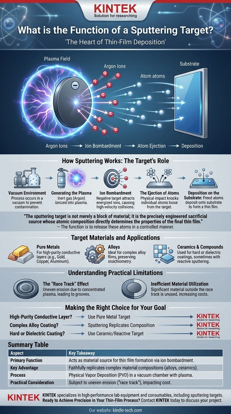
How Sputtering Works: The Target's Role
The function of the sputtering target is best understood as a critical step in a larger, highly controlled physical process known as physical vapor deposition (PVD).
The Vacuum Environment
First, the entire process takes place in a vacuum chamber. This is essential to remove air and other particles that could contaminate the final film or interfere with the process.
Generating the Plasma
An inert gas, most commonly argon, is introduced into the chamber. An electric field is then applied, which energizes the gas and strips electrons from the argon atoms, creating a glowing, ionized gas known as a plasma.
Ion Bombardment
The sputtering target is given a negative electrical charge, which causes the positively charged argon ions from the plasma to accelerate and collide with its surface at high velocity.
The Ejection of Atoms
This high-energy collision is the core of the "sputtering" phenomenon. The impact transfers momentum from the argon ion to the target material, knocking loose or "sputtering" individual atoms from the target's surface. This is a purely physical ejection, not a chemical or thermal one.
Deposition on the Substrate
These newly freed atoms from the target travel through the vacuum chamber and land on the surface of a substrate (such as a semiconductor wafer, glass, or medical implant), gradually building up a thin, uniform film.
Target Materials and Applications
The versatility of sputtering is directly tied to the wide range of materials that can be made into a target. The composition of the target dictates the composition of the final film.
A Versatile Material Palette
Targets can be made from an extensive list of materials, including:
- Pure metals like gold, silver, copper, and aluminum.
- Alloys such as stainless steel.
- Ceramics and compounds like metal oxides or nitrides.
Key Advantage for Complex Materials
Sputtering is especially valuable for depositing materials with very high melting points or for creating complex alloy films. Unlike thermal evaporation, which can struggle with materials that have different boiling points, sputtering ejects atoms in the same ratio as they exist in the target, preserving the alloy's composition.
Understanding the Practical Limitations
While powerful, the sputtering process has practical realities tied directly to the target that engineers must manage for cost, efficiency, and quality.
The "Race Track" Effect
In many systems, magnets are used behind the target to confine the plasma near the surface, increasing the sputtering rate. This concentrates the ion bombardment in a specific ring or oval pattern, causing the target to erode unevenly in a groove often called a "race track."
Inefficient Material Utilization
Because of the race track effect, a significant portion of the target material outside this groove is left unused. This reduces the target utilization, meaning a target must be replaced long before all of its material is consumed, impacting the overall cost of the process.
Target Geometry and Integrity
The target must be large enough to completely cover the plasma erosion zone. If it is too small, the ions can miss the target and instead sputter parts of the sputtering gun itself, such as bearings or clamps, which introduces metallic contamination into the thin film.
Making the Right Choice for Your Goal
The selection and management of the sputtering target are fundamental to achieving the desired outcome of the coating process.
- If your primary focus is a high-purity conductive layer: You must use a target made of a pure metal (e.g., copper, gold) with the highest possible purity to ensure the film's electrical properties are not compromised.
- If your primary focus is a complex alloy coating: Sputtering is the ideal method, as the composition of the target is faithfully replicated in the deposited film, maintaining the desired stoichiometry of the alloy.
- If your primary focus is a hard or dielectric coating: You will use a ceramic target or employ "reactive sputtering," where a gas like oxygen or nitrogen is added to the chamber to react with the sputtered metal atoms as they deposit.
Ultimately, controlling the sputtering target is the key to controlling the composition, quality, and efficiency of your entire thin-film deposition process.
Summary Table:
| Aspect | Key Takeaway |
|---|---|
| Primary Function | Acts as the material source, releasing atoms via ion bombardment to form a thin film on a substrate. |
| Key Advantage | Faithfully replicates complex material compositions (alloys, ceramics) from the target to the film. |
| Process | Physical Vapor Deposition (PVD) in a vacuum chamber using plasma and inert gas (e.g., Argon). |
| Practical Consideration | Subject to uneven erosion ("race track" effect), impacting material utilization and cost. |
Ready to Achieve Precision in Your Thin-Film Process?
Your sputtering target is the heart of your deposition system, directly determining the quality and properties of your final coating. Choosing the right target material and supplier is critical for success.
KINTEK specializes in high-performance lab equipment and consumables, including sputtering targets. We provide the materials and expertise to help you:
- Deposit high-purity conductive layers with pure metal targets.
- Create complex alloy coatings with precise stoichiometry.
- Apply hard, durable ceramic coatings for demanding applications.
Let our experts help you select the ideal target for your specific needs. Contact KINTEK today to discuss your project and ensure optimal results for your laboratory.
Visual Guide
Related Products
- Reference Electrode Calomel Silver Chloride Mercury Sulfate for Laboratory Use
- Multifunctional Electrolytic Electrochemical Cell Water Bath Single Layer Double Layer
- Molybdenum Tungsten Tantalum Special Shape Evaporation Boat
- Hemispherical Bottom Tungsten Molybdenum Evaporation Boat
- Cylindrical Press Mold with Scale for Lab
People Also Ask
- What is the reference electrode in potentiometry? The Key to Stable & Accurate Measurements
- What is the recommended maintenance for the filling solution of a reference electrode? A Guide to Stable & Accurate Readings
- Which electrode is used as a reference electrode for measuring half-cell potentials? Understanding the Universal Standard
- Which electrode is used as a ground reference? Master the Key to Accurate Electrochemical Measurements
- What is the purpose of the reference electrode? Achieve Stable & Accurate Electrochemical Measurements


