The significance of sputtering lies in its ability to create exceptionally durable, uniform, and precisely engineered thin films. It is a physical deposition process where atoms are ejected from a target material and deposited onto a substrate, forming an atomic-level bond that is fundamental to manufacturing high-performance components in industries from semiconductors to optics.
Sputtering is not merely a coating technique; it is a foundational process for building materials from the atom up. Its true significance is providing unparalleled control over a film's properties and creating a bond with the substrate that is often stronger and more reliable than any other deposition method.
How Sputtering Achieves Unmatched Film Quality
To understand why sputtering is so significant, we must first look at its underlying mechanism. Unlike chemical or thermal processes, sputtering is a purely physical phenomenon that provides distinct advantages.
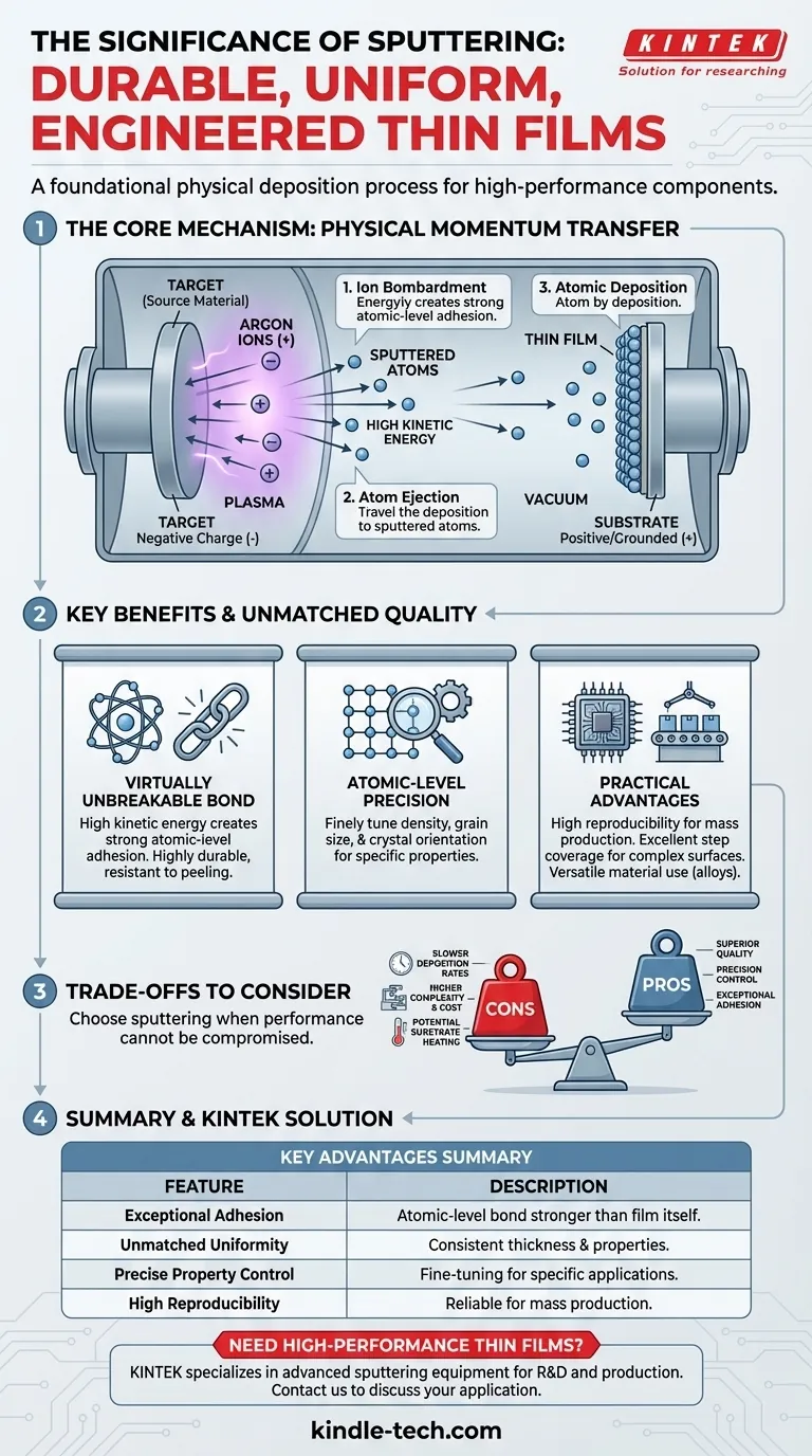
The Core Mechanism: Physical Momentum Transfer
Sputtering begins in a vacuum chamber filled with an inert gas, like Argon. A high voltage is applied to the source material (the target), causing the gas to form a plasma.
Positively charged Argon ions from the plasma are accelerated with immense force into the negatively charged target. This high-energy collision physically knocks out, or "sputters," atoms from the target.
These ejected atoms travel through the vacuum and deposit onto the substrate, building a thin film one atom at a time.
Creating a "Virtually Unbreakable" Bond
The sputtered atoms arrive at the substrate with significant kinetic energy. This energy allows them to form an incredibly strong, dense bond at the atomic level.
This process creates a strong adhesion between the film and the substrate that is almost impossible to break. The result is a coating that is highly durable and resistant to peeling or flaking.
Achieving Atomic-Level Precision
Because sputtering is a highly controllable physical process, it allows for precise manipulation of the final film's characteristics.
Engineers can finely tune the film’s density, grain size, and crystalline orientation by adjusting parameters like gas pressure and power. This level of control is critical for creating materials with specific electrical, optical, or protective properties.
The Practical Advantages in Manufacturing
The physical principles of sputtering translate directly into tangible benefits for industrial and scientific applications, making it a highly reproducible and versatile technique.
High Reproducibility for Mass Production
Sputtering systems offer excellent control over deposition rates and film thickness. This repeatability, combined with the low frequency of target replacement, makes the process extremely reliable and compatible with mass production.
Versatility in Materials
The process is not limited to pure elements. Alloy films can be deposited by using alloy targets or multiple targets simultaneously, allowing for the creation of materials with custom-designed properties that would otherwise be difficult to produce.
Excellent Step Coverage
Sputtered atoms deposit over the substrate from various angles, allowing them to coat complex, non-flat surfaces evenly. This excellent step coverage is crucial for manufacturing microelectronics and other intricate components.
Understanding the Trade-offs
No process is perfect. While sputtering offers superior film quality, its advantages come with certain trade-offs that must be considered.
Slower Deposition Rates
Compared to methods like thermal evaporation, sputtering is often a slower process. The rate of material deposition is typically lower, which can increase process time for very thick films.
Higher Equipment Complexity
Sputtering systems require sophisticated equipment, including vacuum chambers, high-voltage power supplies, and precise gas management systems. This makes the initial investment and operational complexity higher than simpler coating techniques.
Potential for Substrate Heating
The constant bombardment of energetic particles can transfer a significant amount of heat to the substrate. This can be a limiting factor when coating heat-sensitive materials, such as certain plastics or biological samples, and may require additional cooling systems.
Making the Right Choice for Your Goal
Selecting a deposition method depends entirely on the required properties of the final product. Sputtering is the definitive choice when performance cannot be compromised.
- If your primary focus is film durability and adhesion: Sputtering is the superior choice due to its high-energy, physical bonding process that creates an exceptionally strong interface.
- If your primary focus is precise control over film properties: The sputtering process offers unmatched control over factors like density, uniformity, and crystalline structure.
- If your primary focus is high-speed, low-cost deposition for less demanding applications: You may evaluate other methods like thermal evaporation, accepting a trade-off in film density and adhesion.
Ultimately, sputtering's significance lies in its power to construct high-performance films with a level of quality and control that is foundational to modern technology.
Summary Table:
| Key Advantage | Description |
|---|---|
| Exceptional Adhesion | Creates an atomic-level bond stronger than the film itself, preventing peeling. |
| Unmatched Uniformity | Deposits atoms evenly for highly consistent film thickness and properties. |
| Precise Property Control | Allows fine-tuning of density, grain size, and structure for specific applications. |
| High Reproducibility | Ideal for mass production with reliable, repeatable results. |
| Versatile Material Use | Capable of depositing pure metals, alloys, and compounds from various targets. |
Need to deposit a high-performance thin film?
If your project demands a coating with superior adhesion, precise control, and exceptional durability, sputtering is the definitive solution. KINTEK specializes in providing advanced sputtering equipment and consumables tailored to the exacting needs of R&D and production laboratories.
Let our experts help you select the right system to achieve the material properties critical to your success.
Contact KINTALK today to discuss your specific application requirements.
Visual Guide