In essence, sputtering is a physical process used to deposit exceptionally thin films of a metal onto a surface. It works by bombarding a solid block of the source metal, called a "target," with energized ions of an inert gas inside a vacuum. This atomic-scale bombardment is energetic enough to knock loose individual atoms from the target, which then fly across the chamber and coat a desired object, or "substrate," layer by atomic layer.
Sputtering is best understood as a controlled form of atomic erosion. By using a plasma to create high-energy ion "projectiles," you can precisely chip away atoms from a source material and redeposit them to form a high-quality, ultra-thin coating on another surface.
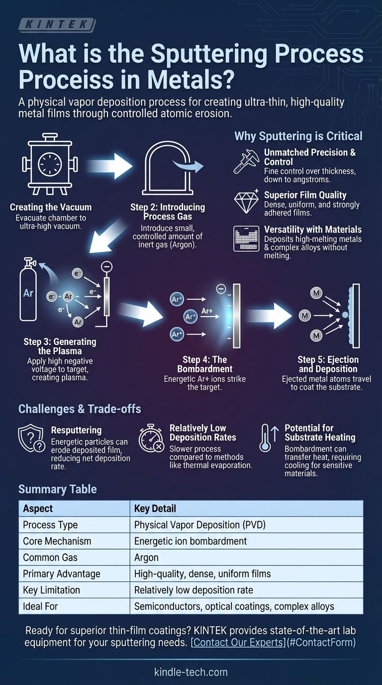
The Mechanics of Sputtering: A Step-by-Step Guide
The sputtering process is a highly controlled sequence that takes place entirely within a specialized vacuum chamber. Each step is critical to achieving a uniform and pure thin film.
Step 1: Creating the Vacuum
First, the chamber is evacuated to an ultra-high vacuum. This removes ambient air and other contaminants that could otherwise react with the metal atoms or interfere with their path to the substrate.
Step 2: Introducing the Process Gas
A small, precisely controlled amount of an inert gas, most commonly argon, is then introduced into the chamber. This gas is not meant to react chemically; it will be used to create the projectiles for bombardment.
Step 3: Generating the Plasma
A high negative voltage is applied to the metal target. This strong electrical field accelerates free electrons, causing them to collide with the neutral argon atoms. These collisions knock electrons off the argon atoms, turning them into positively charged ions and creating a sustained, glowing plasma.
Step 4: The Bombardment
The newly formed positive argon ions are now strongly attracted and accelerated toward the negatively charged metal target. They strike the target's surface with significant kinetic energy.
Step 5: Ejection and Deposition
This energetic impact transfers momentum to the metal atoms on the surface of the target, giving them enough energy to escape, or be "sputtered." These ejected metal atoms travel in a straight line through the vacuum until they land on the substrate, gradually building up a thin, even film.
Why Sputtering is a Critical Industrial Process
Sputtering is not just a laboratory curiosity; it is a cornerstone of modern manufacturing, especially in electronics and optics, due to its unique advantages.
Unmatched Precision and Control
The process allows for exceptionally fine control over the thickness of the deposited film, often down to the scale of single angstroms (tenths of a nanometer). This is critical for manufacturing complex semiconductor devices, optical filters, and hard drive platters.
Superior Film Quality
Because the sputtered atoms arrive at the substrate with high kinetic energy, they form very dense, uniform, and strongly adhered films. This results in coatings that are more durable and have better performance characteristics than those created by some alternative methods.
Versatility with Materials
Sputtering is a purely physical process, not a thermal one. It does not require melting the source material, making it ideal for depositing metals with extremely high melting points (like tungsten or tantalum) or for creating films from complex alloys whose composition must be preserved.
Understanding the Trade-offs and Challenges
While powerful, sputtering is not a universal solution. Understanding its limitations is key to using it effectively.
The Problem of Resputtering
The same energetic environment that makes sputtering work can also be a drawback. The deposited film on the substrate can itself be bombarded by energetic particles in the plasma, causing already-deposited atoms to be knocked loose. This phenomenon, known as resputtering, can reduce the net deposition rate and alter the film's properties if not properly managed.
Relatively Low Deposition Rates
Compared to other methods like thermal evaporation, sputtering can be a slower process. The rate at which material is transferred is often lower, making it less suitable for applications requiring very thick coatings or high-speed, bulk deposition.
Potential for Substrate Heating
The constant bombardment of energetic particles can transfer a significant amount of heat to the substrate. This can be problematic when coating temperature-sensitive materials like plastics or certain organic electronic components, requiring active cooling systems.
Making the Right Choice for Your Goal
Selecting a deposition method depends entirely on the required properties of the final film and your manufacturing constraints.
- If your primary focus is creating a highly uniform, dense, and strongly adhered film: Sputtering is an excellent choice due to the energetic nature of the deposited atoms.
- If your primary focus is coating with complex alloys or refractory metals with high melting points: Sputtering is often superior to thermal methods because it does not require melting the source material.
- If your primary focus is rapid, bulk coating where ultimate film quality is secondary: You should evaluate sputtering against faster methods like thermal evaporation, weighing the trade-off between deposition speed and film density.
By understanding sputtering as a process of controlled atomic transfer, you can better leverage its precision for advanced material engineering and surface modification.
Summary Table:
| Aspect | Key Detail |
|---|---|
| Process Type | Physical Vapor Deposition (PVD) |
| Core Mechanism | Energetic ion bombardment of a target material |
| Common Process Gas | Argon |
| Primary Advantage | High-quality, dense, and uniform films |
| Key Limitation | Relatively low deposition rate |
| Ideal For | Semiconductors, optical coatings, complex alloys |
Ready to achieve superior thin-film coatings for your laboratory?
Sputtering is a cornerstone of modern material science, enabling the creation of high-performance, ultra-thin films essential for advanced research and development. KINTEK specializes in providing state-of-the-art lab equipment and consumables tailored to your precise deposition needs.
Whether you are working on semiconductor devices, optical components, or novel alloy coatings, our expertise ensures you have the right tools for unparalleled precision and film quality.
Contact our experts today to discuss how our sputtering solutions can enhance your laboratory's capabilities and drive your projects forward.
Visual Guide
Related Products
- Spark Plasma Sintering Furnace SPS Furnace
- Vacuum Induction Melting Spinning System Arc Melting Furnace
- Chemical Vapor Deposition CVD Equipment System Chamber Slide PECVD Tube Furnace with Liquid Gasifier PECVD Machine
- Customer Made Versatile CVD Tube Furnace Chemical Vapor Deposition Chamber System Equipment
People Also Ask
- What is the pressure for spark plasma sintering? A Guide to Optimizing SPS Parameters
- Why are Spark Plasma Sintering (SPS) furnaces or hot presses utilized in the preparation of Li3PS4 solid electrolytes?
- What are the fundamentals of spark plasma sintering process? Unlock Rapid, High-Performance Material Consolidation
- What is the difference between spark plasma sintering and flash sintering? A Guide to Advanced Sintering Methods
- What are the advantages of CAMI/SPS for W-Cu composite preparation? Reduce cycles from hours to seconds.


