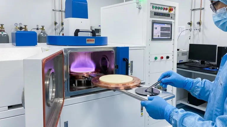
In materials science and semiconductor fabrication, a gallium oxide (Ga₂O₃) sputtering target is a solid, high-purity source material used to create thin films. Typically formed into a dense ceramic disc or plate, this target is placed inside a vacuum chamber where it is bombarded by energetic ions in a process called sputtering, which deposits a layer of gallium oxide onto a substrate.
The quality of a gallium oxide sputtering target—specifically its purity, density, and composition—is not a minor detail. It is the single most critical factor that dictates the performance, quality, and reproducibility of the final Ga₂O₃ thin film used in advanced electronic and optoelectronic devices.
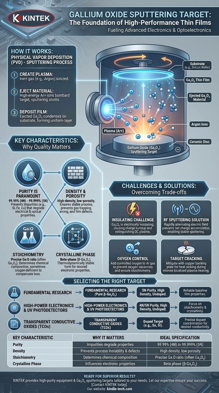
How Sputtering with a Gallium Oxide Target Works
To understand the target's importance, you must first understand its role in the Physical Vapor Deposition (PVD) process known as sputtering.
The Sputtering Process Explained
The process begins by creating a plasma, typically from an inert gas like argon, within a vacuum chamber. A high voltage is applied, which ionizes the argon gas atoms.
Ejecting the Material
These positively charged argon ions are accelerated toward the negatively biased gallium oxide target. The high-energy impact physically knocks out, or "sputters," atoms and molecules from the target's surface.
Deposition onto the Substrate
The ejected Ga₂O₃ material travels across the vacuum chamber and condenses on a substrate, such as a silicon wafer or sapphire crystal. This gradually builds a thin, uniform film of gallium oxide.
Key Characteristics of a High-Quality Ga₂O₃ Target
The properties of the starting target are directly transferred to the deposited film. Therefore, sourcing a high-quality target is non-negotiable for achieving high-performance results.
Purity is Paramount
Any metallic or non-metallic impurities within the target (e.g., Si, Fe, Cu) will be co-deposited into your film. These impurities can act as charge traps or scattering centers, severely degrading the film's electrical and optical properties. High purity (typically 99.99% or 4N, and up to 99.999% or 5N) is essential.
Density and Porosity
A high-density, low-porosity target is crucial for a stable and repeatable process. Voids or pores within the ceramic can trap gas, leading to uncontrolled pressure bursts and process instability. This can cause arcing or "spitting," which generates defects in the film. High density ensures a consistent sputtering rate.
Stoichiometry and Composition
The target must have the correct chemical ratio of gallium to oxygen. While pure stoichiometric Ga₂O₃ is standard, sometimes targets are intentionally fabricated to be slightly oxygen-deficient to compensate for oxygen loss during the sputtering process.
Crystalline Phase
Gallium oxide can exist in several different crystalline structures (polymorphs). The most thermodynamically stable and widely studied is the beta-phase (β-Ga₂O₃). Most high-quality targets are made from β-Ga₂O₃ powder to promote the growth of this phase in the final film.
Understanding the Trade-offs and Challenges
Sputtering gallium oxide is not without its difficulties. Its material properties present specific challenges that must be addressed at the process level.
The Challenge of Insulating Materials
As a wide-bandgap semiconductor, gallium oxide is highly electrically insulating at room temperature. Using a standard Direct Current (DC) sputtering power supply will cause positive charge to build up on the target's surface, repelling the incoming argon ions and quickly extinguishing the plasma.
The RF Sputtering Solution
The industry-standard solution is to use Radio Frequency (RF) sputtering. The rapidly alternating electric field (typically at 13.56 MHz) prevents net charge accumulation, allowing for the continuous and stable sputtering of insulating materials like Ga₂O₃.
Controlling Oxygen Content
The high-energy sputtering process can break Ga-O bonds, and some oxygen may be lost to the vacuum pump. This creates oxygen vacancies in the deposited film, which can unintentionally make it electrically conductive (n-type). To counteract this, a controlled amount of oxygen is often added to the argon sputtering gas to ensure the final film has the desired stoichiometry and insulating properties.
Target Cracking
Ga₂O₃ is a brittle ceramic material with low thermal conductivity. The intense, localized heating from plasma bombardment can create thermal stress, leading to target cracking. This is mitigated by bonding the target to a copper backing plate, which acts as a heat sink to improve cooling.
Selecting the Right Gallium Oxide Target
The specific type of Ga₂O₃ target you need depends entirely on the intended application of your thin film.
- If your primary focus is fundamental research on pure β-Ga₂O₃: Opt for the highest purity (5N) undoped target with the highest possible density to establish a reliable baseline for film properties.
- If your primary focus is developing UV photodetectors or high-power electronics: Prioritize a high-purity (4N or 5N), high-density undoped target and focus your process control on managing stoichiometry and crystallinity.
- If your primary focus is creating transparent conductive oxides (TCOs): You must use a doped target, such as tin-doped (GTO) or silicon-doped Ga₂O₃, with a precisely specified dopant concentration to achieve the desired conductivity.
Ultimately, the sputtering target is not just a source material; it is the foundational blueprint for your final thin-film device.
Summary Table:
| Key Characteristic | Why It Matters | Ideal Specification |
|---|---|---|
| Purity | Impurities degrade electrical/optical film properties. | 99.99% (4N) to 99.999% (5N) |
| Density | Prevents process instability, arcing, and film defects. | High density, low porosity |
| Stoichiometry | Determines the chemical composition of the final film. | Precise Ga:O ratio (often Ga₂O₃) |
| Crystalline Phase | Influences the electronic properties of the deposited film. | Beta-phase (β-Ga₂O₃) is standard |
Ready to achieve superior thin-film results with a high-quality gallium oxide sputtering target? The foundational blueprint for your advanced electronic or optoelectronic device starts with the right source material. KINTEK specializes in providing high-purity lab equipment and consumables, including precisely engineered Ga₂O₃ sputtering targets tailored to your research or production needs—whether for high-power electronics, UV photodetectors, or transparent conductive oxides. Let our expertise ensure your process stability and film performance. Contact KINTEK today to discuss your specific requirements and elevate your laboratory's capabilities.
Visual Guide
Related Products
- Laboratory CVD Boron Doped Diamond Materials
- Boron Nitride (BN) Ceramic Plate
- Engineering Advanced Fine Ceramics Alumina Crucibles (Al2O3) for Thermal Analysis TGA DTA
- Hemispherical Bottom Tungsten Molybdenum Evaporation Boat
- Optical Window Glass Substrate Wafer Quartz Plate JGS1 JGS2 JGS3
People Also Ask
- Are CVD diamonds synthetic? Discover the Truth About Lab-Grown Diamonds
- What is the purpose of adding a boron source in CVD diamond growth? Master P-Type Semiconductor Conductivity
- What are the applications of CVD diamonds? From Jewelry to High-Tech Tools
- What materials are CVD deposition? From Semiconductors to Super-Hard Coatings
- What is the demand of CVD diamonds? Driven by Ethics, Purity, and Affordability