In principle, nearly any material can be sputter coated, but in practice, the most commonly used materials are conductive metals and their alloys. The process is most frequently associated with noble metals like gold (Au), platinum (Pt), and gold/palladium (Au/Pd) blends, which are chosen for their excellent electrical conductivity and resistance to oxidation.
While many materials can be used for sputter coating, the choice is not arbitrary. The ideal material is a strategic decision dictated by your analytical goal—whether it's achieving the highest image resolution, ensuring accurate elemental analysis, or simply preparing a sample for standard imaging.
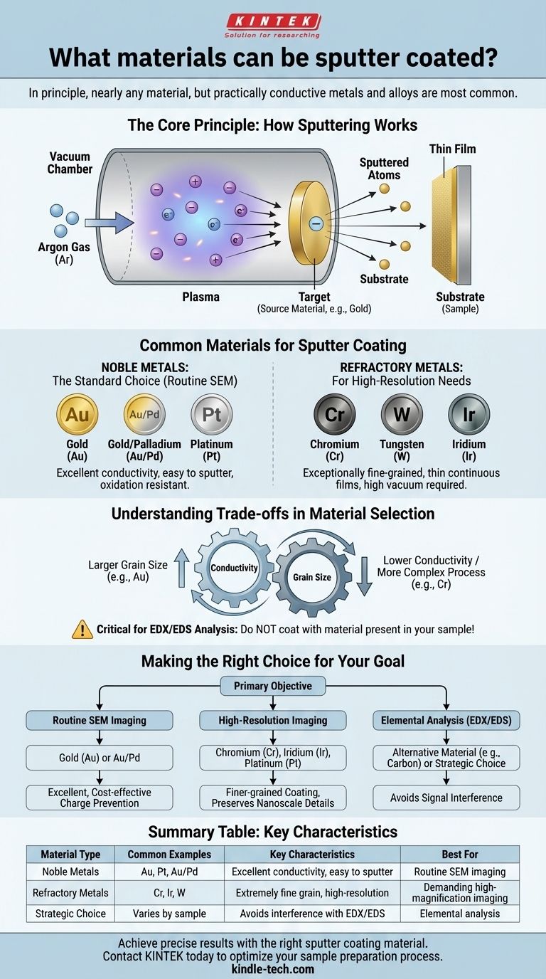
The Core Principle: How Sputtering Works
To understand which materials are suitable, you must first understand the mechanism. Sputter coating is a physical vapor deposition (PVD) process that occurs within a vacuum chamber.
Creating a Plasma in a Vacuum
The process begins by introducing a high-purity inert gas, almost always argon (Ar), into a low-pressure vacuum chamber. An electric field is applied, which ionizes the argon gas atoms and transforms them into a glowing plasma of positively charged ions.
Bombarding the Target
These positively charged argon ions are then accelerated by the electric field toward a negatively charged plate known as the target. This target is made of the material you wish to use for the coating (e.g., a solid disc of pure gold).
Deposition on the Substrate
When the high-energy ions strike the target, their momentum is sufficient to dislodge or "sputter" individual atoms from the target's surface. These ejected atoms travel in straight lines until they strike your sample (the substrate), gradually building up a thin, uniform film.
Common Materials for Sputter Coating
The material chosen for the target directly impacts the quality and characteristics of the final coating. Materials are generally selected based on conductivity, grain size, and chemical inertness.
Noble Metals: The Standard Choice
For general-purpose applications, especially preparing non-conductive samples for Scanning Electron Microscopy (SEM), noble metals are the default.
- Gold (Au): Highly conductive and easy to sputter, making it an excellent all-around choice for preventing charge build-up on a sample surface.
- Gold/Palladium (Au/Pd): This alloy produces a slightly finer grain structure than pure gold, offering a good balance between performance and cost.
- Platinum (Pt): Also provides a fine-grained coating and is extremely resistant to oxidation, making it a premium choice for many applications.
Refractory Metals: For High-Resolution Needs
When imaging at very high magnifications, the grain size of the coating itself can obscure the fine details of your sample. In these cases, materials that form smaller grains are required.
- Chromium (Cr): Known for producing exceptionally fine-grained and thin continuous films, making it ideal for high-resolution imaging. Sputtering chromium effectively requires a higher-quality vacuum than what is needed for gold.
- Tungsten (W) or Iridium (Ir): These materials also offer extremely fine grain structures and are used for the most demanding high-resolution applications.
Understanding the Trade-offs in Material Selection
Choosing a material involves balancing performance characteristics against your specific analytical requirements. There is no single "best" material for all situations.
Conductivity vs. Grain Size
There is often a trade-off between electrical conductivity and grain size. Gold is an excellent conductor but tends to form larger grains, which can limit ultimate image resolution. Chromium provides a much finer structure but may require more careful process control to achieve a perfectly conductive layer.
Material Compatibility and Analysis
This is a critical consideration often overlooked by beginners. If you plan to perform elemental analysis on your sample using techniques like Energy-Dispersive X-ray Spectroscopy (EDX/EDS), you must not coat the sample with a material that is also present in your sample. For example, coating a gold nanoparticle sample with gold makes it impossible to distinguish the coating from the sample itself.
Process Requirements
Your choice of material is constrained by your equipment. As noted, sputtering finer-grained materials like chromium often requires a more advanced vacuum system (like a turbomolecular pump) compared to the simpler rotary pumps sufficient for gold sputtering.
Making the Right Choice for Your Goal
Select your coating material based on a clear understanding of your primary objective.
- If your primary focus is routine SEM imaging: A Gold (Au) or Gold/Palladium (Au/Pd) coating provides excellent, cost-effective charge prevention with a straightforward process.
- If your primary focus is high-resolution imaging: Choose Chromium (Cr), Iridium (Ir), or Platinum (Pt) to produce a finer-grained coating that preserves nanoscale surface features.
- If your primary focus is elemental analysis (EDX/EDS): Use a coating material not present in your sample, or consider an alternative like carbon coating (typically done via evaporation) to provide conductivity without metallic signal interference.
Ultimately, a deliberate material choice transforms sputter coating from a simple preparation step into a powerful tool for achieving precise and reliable analytical results.
Summary Table:
| Material Type | Common Examples | Key Characteristics | Best For |
|---|---|---|---|
| Noble Metals | Gold (Au), Platinum (Pt), Au/Pd | Excellent conductivity, easy to sputter | Routine SEM imaging, charge prevention |
| Refractory Metals | Chromium (Cr), Iridium (Ir) | Extremely fine grain, high-resolution | Demanding high-magnification imaging |
| Strategic Choice | Varies by sample | Avoids interference with EDX/EDS analysis | Elemental analysis without signal overlap |
Achieve precise and reliable results with the right sputter coating material. The choice between gold for routine conductivity or chromium for high-resolution detail is critical for your lab's success. At KINTEK, we specialize in providing high-quality lab equipment and consumables tailored to your specific analytical needs. Our experts can help you select the ideal sputter coating solution to enhance your SEM imaging and analysis. Contact us today to discuss your requirements and optimize your sample preparation process.
Get in touch with our specialists
Visual Guide