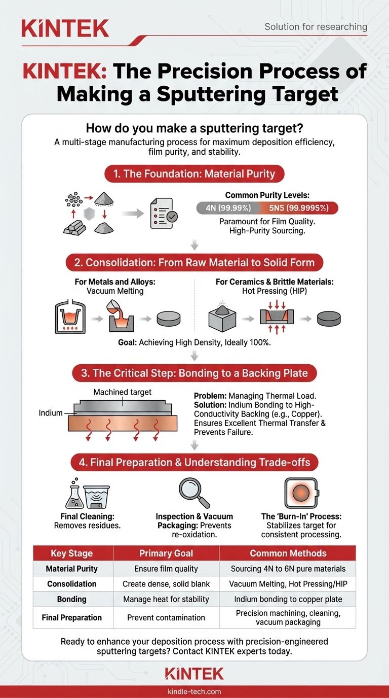
Making a sputtering target is a precise, multi-stage manufacturing process that goes far beyond simply shaping a piece of metal. It begins with sourcing exceptionally pure raw materials, which are then consolidated into a dense, solid form. This solid blank is machined to exact specifications, bonded to a heat-dissipating backing plate, and then meticulously cleaned and packaged to prevent contamination before use.
The quality of a sputtering target is not defined by a single step, but by a chain of precision processes. From raw material purity to final bonding, each stage is engineered to ensure maximum deposition efficiency, film purity, and stability within the demanding environment of a vacuum chamber.
The Foundation: Material Purity
Why Purity is Paramount
The sputtering process transfers material from the target to your substrate on an atomic level. Any impurity present in the target, whether it's a stray element or an oxide, has the potential to be transferred into your thin film, compromising its electrical, optical, or mechanical properties.
Starting with high-purity material is the non-negotiable first step.
Common Purity Levels
Target purity is often described in "nines." For example, "4N" purity means 99.99% pure, while "5N5" means 99.9995% pure. The required purity level is dictated entirely by the sensitivity of the final application, with semiconductor and optical coatings demanding the highest grades.
From Raw Material to Solid Form
For Metals and Alloys: Vacuum Melting
The most common method for metallic targets is melting the high-purity raw materials (ingots, granules, or powders) in a vacuum or inert gas environment. This prevents the material from reacting with oxygen or other atmospheric contaminants. The molten material is then cast into a mold to create a dense, solid "blank."
For Ceramics and Brittle Materials: Hot Pressing
Ceramic or other brittle materials that cannot be easily melted are typically formed from high-purity powders. The powder is loaded into a graphite die and simultaneously subjected to immense pressure and high temperature. This process, known as hot pressing or hot isostatic pressing (HIP), sinters the powder into a fully dense, solid form.
The Goal: Achieving High Density
Regardless of the method, the primary goal is to create a target blank with the highest possible density, ideally close to 100% of the material's theoretical density. Low-density areas or voids can lead to uneven sputtering, particle generation, and arcing during the process.
The Critical Step: Bonding to a Backing Plate
The Problem: Managing Thermal Load
The sputtering process is thermally inefficient. The bombardment of ions generates a tremendous amount of heat in the target. If this heat is not effectively removed, the target can overheat, leading to warping, cracking, or changes in its microstructure, all of which disrupt the deposition process.
The Solution: Bonding
To solve this, the machined target is bonded to a backing plate, which is typically made of a high thermal conductivity material like oxygen-free copper (OFC). The most common bonding method uses a thin layer of Indium alloy. The target and backing plate are heated in a vacuum, allowing the indium to melt and form a uniform, void-free bond that ensures excellent thermal transfer.
Why Bonding Prevents Target Failure
A proper bond is the single most important factor for target lifespan and performance. It allows cooling water, flowing through channels in the sputtering gun (magnetron), to efficiently draw heat away from the target face via the backing plate.
Understanding the Trade-offs and Final Steps
Monolithic vs. Bonded Targets
Some robust, metallic materials can be fabricated as a single piece, or "monolithic," where the target and mounting features are machined from one block. However, for the vast majority of materials, especially ceramics or precious metals, a bonded assembly is the standard, as it conserves expensive material and ensures superior thermal management.
The "Burn-In" Process
Even a perfectly manufactured target requires conditioning. When a fresh target is installed, microscopic surface oxides and adsorbed gases can cause instability and arcing. The "burn-in" process, as mentioned in the references, involves running the target at low power and gradually ramping it up. This gently sputters away the initial surface layer, stabilizing the target for consistent processing.
Final Cleaning and Packaging
The final step is a multi-stage cleaning process to remove any oils or residues from machining and bonding. The target is then inspected for quality and vacuum-sealed in cleanroom-grade packaging to prevent re-oxidation before it reaches you.
Making the Right Choice for Your Process
- If your primary focus is process stability and long lifespan: Prioritize targets with documented high density and a void-free indium bond to a well-designed backing plate.
- If your primary focus is film purity for sensitive applications: Specify the highest available material purity (e.g., 5N or 6N) and confirm the manufacturer uses rigorous final cleaning and vacuum packaging protocols.
- If you are experiencing issues like arcing, cracking, or inconsistent rates: Investigate the target's bonding integrity and density, and ensure a proper burn-in procedure is being followed for every new target.
Ultimately, understanding how a sputtering target is made empowers you to select the right component and troubleshoot your deposition process with precision.
Summary Table:
| Key Manufacturing Stage | Primary Goal | Common Methods |
|---|---|---|
| Material Purity | Ensure film quality by minimizing impurities | Sourcing 4N (99.99%) to 6N (99.9999%) pure materials |
| Consolidation | Create a dense, solid blank | Vacuum Melting (metals), Hot Pressing/HIP (ceramics) |
| Bonding | Manage heat for process stability and lifespan | Indium bonding to a copper backing plate |
| Final Preparation | Prevent contamination and ensure performance | Precision machining, meticulous cleaning, vacuum packaging |
Ready to enhance your deposition process with precision-engineered sputtering targets?
At KINTEK, we specialize in manufacturing high-purity lab equipment and consumables, including sputtering targets tailored to your specific application—whether for semiconductors, optics, or research. Our targets are engineered for maximum density, superior bonding, and consistent performance to ensure film purity and process stability.
Contact our experts today to discuss your requirements and discover how our targets can improve your lab's efficiency and results.
Get a Quote & Discuss Your Needs
Visual Guide
Related Products
- Reference Electrode Calomel Silver Chloride Mercury Sulfate for Laboratory Use
- Multifunctional Electrolytic Electrochemical Cell Water Bath Single Layer Double Layer
- Molybdenum Tungsten Tantalum Special Shape Evaporation Boat
- Hemispherical Bottom Tungsten Molybdenum Evaporation Boat
- Cylindrical Press Mold with Scale for Lab
People Also Ask
- What is the purpose of the reference electrode? Achieve Stable & Accurate Electrochemical Measurements
- Which electrode is used as a reference? A Guide to Accurate Electrochemical Measurements
- How does the selection of reference electrodes correlate with electrolyte pH in HER testing? Ensure Precise Potential
- Which electrode is used as a ground reference? Master the Key to Accurate Electrochemical Measurements
- Which type of electrode can be used as a reference point? Select the Right One for Accurate Measurements


