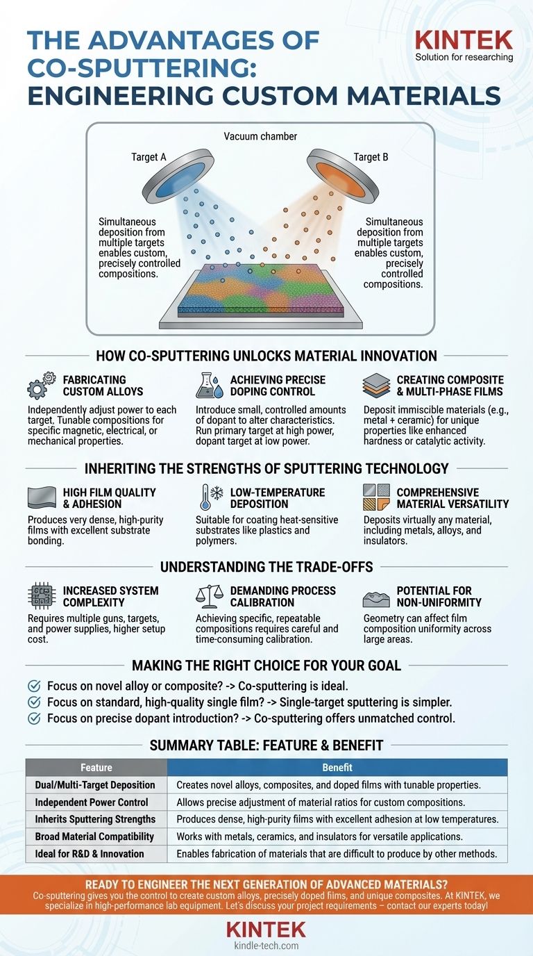
The primary advantage of co-sputtering is its unique ability to create films with custom, precisely controlled compositions. Instead of depositing a single material, co-sputtering uses two or more targets to simultaneously deposit different materials onto a substrate. This allows for the fabrication of novel alloys, doped films, and composite materials that would be difficult or impossible to create using a single-source deposition method.
Co-sputtering moves beyond simply coating a surface with a pre-existing material. It transforms the deposition process into an act of material engineering, allowing you to build entirely new materials with tailored properties directly on the substrate.
How Co-Sputtering Unlocks Material Innovation
While standard sputtering is excellent for depositing a single material, co-sputtering is a technique specifically designed for creating material mixtures. This opens up a vast range of possibilities for research and industrial applications.
Fabricating Custom Alloys
One of the most powerful uses of co-sputtering is the creation of metallic alloys. Instead of needing a pre-fabricated alloy target, you can use individual targets of the constituent elements (e.g., one of copper, one of zinc to make brass).
By independently adjusting the power supplied to each sputtering gun, you can precisely control the ratio of each element in the final film. This allows for the creation of alloys with a tunable composition, which is invaluable for developing materials with specific magnetic, electrical, or mechanical properties.
Achieving Precise Doping Control
Co-sputtering provides exceptional control for doping—introducing a small, controlled amount of one material into a host material to alter its characteristics.
For example, a primary material target can be run at high power while a second "dopant" target is run at very low power. This allows for the incorporation of dopants with a precision that is difficult to achieve by other means, fundamentally changing the film's semiconductor or optical properties.
Creating Composite and Multi-Phase Films
The technique is not limited to materials that form homogenous alloys. Co-sputtering can be used to deposit immiscible materials, such as a metal and a ceramic, simultaneously.
This results in composite films or nanocomposites, where one material is embedded within a matrix of another. These materials can exhibit unique combinations of properties, such as enhanced hardness, specific optical responses, or catalytic activity.
Inheriting the Strengths of Sputtering Technology
Co-sputtering is not a separate technology but rather a method of using sputtering systems. Therefore, it benefits from all the core advantages of the underlying sputtering process, most commonly magnetron sputtering.
High Film Quality and Adhesion
Like single-target sputtering, co-sputtering produces very dense, high-purity films. The energetic nature of the sputtering process results in excellent adhesion, where the deposited film bonds strongly to the substrate surface.
Low-Temperature Deposition
Sputtering is a low-temperature process compared to thermal evaporation. This makes co-sputtering suitable for coating heat-sensitive substrates, such as plastics, polymers, and certain electronic components, without causing damage.
Comprehensive Material Versatility
The sputtering process can deposit virtually any material, including high-melting-point metals, alloys, and compounds. When combined with RF power supplies, it can also deposit insulators and dielectrics, making co-sputtering a highly versatile tool for nearly any class of material.
Understanding the Trade-offs
While powerful, co-sputtering introduces complexity that is important to acknowledge.
Increased System Complexity
A co-sputtering setup requires multiple sputtering guns, targets, and power supplies within a single vacuum chamber. This makes the system more complex and costly to set up and maintain compared to a single-target system.
Demanding Process Calibration
Achieving a specific, repeatable film composition is not trivial. It requires careful calibration of the deposition rates for each material under various power settings. This calibration can be time-consuming and must be re-verified regularly.
Potential for Non-Uniformity
The geometry of the chamber—the placement of multiple targets relative to the substrate—can affect the uniformity of the film's composition across the substrate area. While this can be engineered to create intentional "compositional gradients" for research, it presents a challenge for achieving uniform coatings over large areas.
Making the Right Choice for Your Goal
Co-sputtering is a specialized technique that offers unparalleled flexibility. Your choice to use it should be driven by your end goal.
- If your primary focus is fabricating a novel alloy or composite material: Co-sputtering is the ideal choice for its compositional flexibility and control.
- If your primary focus is depositing a standard, single-material film with high quality: A simpler single-target sputtering process is more straightforward and cost-effective.
- If your primary focus is introducing a precise amount of a dopant into a film: Co-sputtering offers a level of control that is difficult to match with other methods.
Ultimately, co-sputtering empowers you to treat the vacuum chamber as a laboratory for engineering materials from the atoms up.
Summary Table:
| Feature | Benefit |
|---|---|
| Dual/Multi-Target Deposition | Creates novel alloys, composites, and doped films with tunable properties. |
| Independent Power Control | Allows precise adjustment of material ratios for custom compositions. |
| Inherits Sputtering Strengths | Produces dense, high-purity films with excellent adhesion at low temperatures. |
| Broad Material Compatibility | Works with metals, ceramics, and insulators for versatile applications. |
| Ideal for R&D & Innovation | Enables fabrication of materials that are difficult to produce by other methods. |
Ready to engineer the next generation of advanced materials? Co-sputtering gives you the control to create custom alloys, precisely doped films, and unique composites tailored to your specific research or production needs. At KINTEK, we specialize in providing high-performance lab equipment, including advanced sputtering systems, to support your material science innovations.
Let's discuss your project requirements — contact our experts today to find the perfect co-sputtering solution for your laboratory!
Visual Guide
Related Products
People Also Ask
- What is twin screw granulation? A Guide to Modern, Continuous Pharmaceutical Manufacturing
- What is the screw extrusion process? A Guide to Continuous Plastic Profiling
- What are the disadvantages of twin screw? Higher Cost and Complexity vs. Single Screw
- What are the advantages of twin screw granulation? Achieve Superior Control and Consistency in Manufacturing
- What is twin screw extrusion? Achieve Superior Mixing and Uniform Product Quality