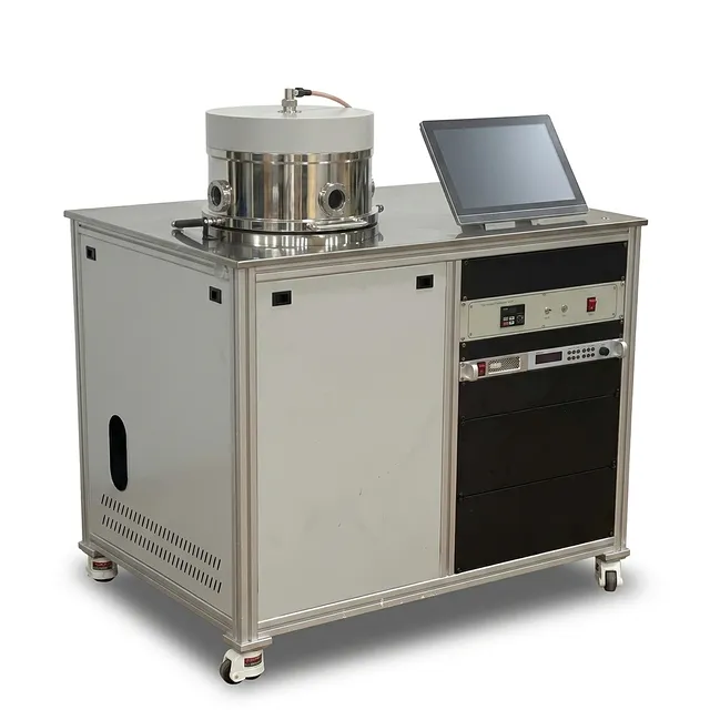
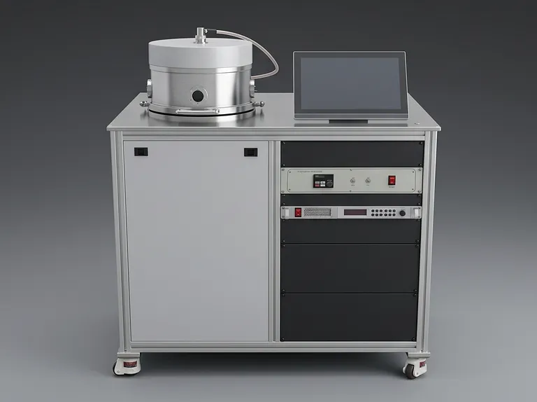
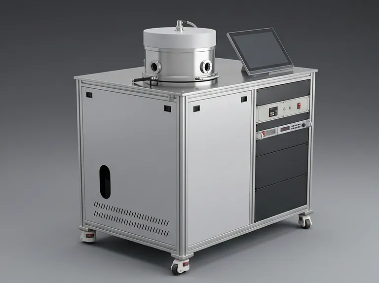
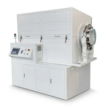
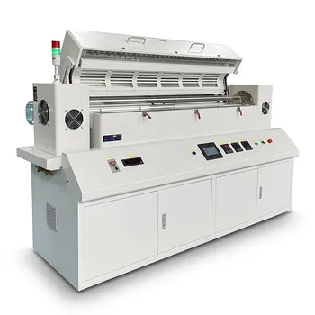
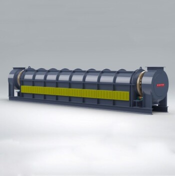
Products Thermal Equipment CVD & PECVD Furnace Plasma enhanced evaporation deposition PECVD coating machine
Plasma enhanced evaporation deposition PECVD coating machine

CVD & PECVD Furnace

Plasma enhanced evaporation deposition PECVD coating machine

Item Number : KT-PED

Price varies based on specs and customizations


Sample holder heating temperature
≤800℃
Gas purge channels
4 channels
Vacuum chamber chamber size
Φ500mm × 550 mm
ISO & CE icon

Shipping:

Contact us to get shipping details Enjoy On-time Dispatch Guarantee.

Introduction

Plasma Enhanced Chemical Vapor Deposition (PECVD) is a vacuum thin film deposition process that uses vapors or gases as precursors to create a coating. PECVD is a variation of chemical vapor deposition (CVD) that uses plasma instead of heat to activate the source gas or vapor. Since high temperatures can be avoided, the range of possible substrates expands to low melting point materials – even plastics in some cases. Moreover, the range of coating materials that can be deposited also grows. PECVD is used to deposit a wide variety of materials, including dielectrics, semiconductors, metals, and insulators. PECVD coatings are used in a wide variety of applications, including solar cells, flat panel displays, and microelectronics.

Applications

Plasma Enhanced Chemical Vapor Deposition (PECVD) coating machines offer a versatile solution for various industries and applications:

  • LED Lighting:** Deposition of high-quality dielectric and semiconductor films for light-emitting diodes (LEDs).
  • Power Semiconductors:** Formation of insulating layers, gate oxides, and other critical components in power semiconductor devices.
  • MEMS:** Fabrication of thin films for microelectromechanical systems (MEMS), such as sensors and actuators.
  • Optical Coatings:** Deposition of anti-reflection coatings, optical filters, and other optical components.
  • Thin Film Solar Cells:** Production of amorphous and microcrystalline silicon thin films for solar cell devices.
  • Surface Modification:** Enhancement of surface properties, such as corrosion resistance, wear resistance, and biocompatibility.
  • Nanotechnology:** Synthesis of nanomaterials, including nanoparticles, nanowires, and thin films.

Plasma enhanced evaporation deposition PECVD coating machine details


Features

The Plasma Enhanced Chemical Vapor Deposition (PECVD) Coating Machine offers numerous advantages that enhance productivity and deliver exceptional results:

  • Low-temperature deposition: Enables the formation of high-quality films at temperatures significantly lower than traditional CVD methods, making it suitable for delicate substrates.
  • High deposition rates: Maximizes efficiency by depositing films rapidly, reducing production time and increasing output.
  • Uniform and crack-resistant films: Ensures consistent film properties and minimizes the risk of cracking, leading to reliable and durable coatings.
  • Excellent adhesion to substrates: Provides strong bonding between the film and the substrate, ensuring long-lasting performance and preventing delamination.
  • Versatile coating capabilities: Allows for the deposition of a wide range of materials, including SiO2, SiNx, and SiOxNy, to meet diverse application requirements.
  • Customization for complex geometries: Accommodates substrates with intricate shapes, ensuring uniform coating and optimal performance.
  • Low maintenance and easy installation: Minimizes downtime and simplifies setup, enhancing productivity and cost-effectiveness.

Technical specifications

Sample holder Size 1-6 inches
Rotate speed 0-20rpm adjustable
Heating temperature ≤800℃
Control accuracy ±0.5℃  SHIMADEN PID Controller
Gas purge Flow meter  MASS FLOWMETER CONTROLLER (MFC)
Channels 4 channels
Cooling method Circulating water cooling
Vacuum chamber Chamber size Φ500mm X 550mm    
Observation port Full view port with baffle
Chamber material 316 Stainless steel
Door type Front open type door
  Cap material 304 Stainless steel
Vacuum pump port CF200 flange
Gas inlet port  φ6 VCR connector
Plasma power Source power DC power or RF power
Coupling mode Inductively coupled or plate capacitive
Output power 500W—1000W
Bias power 500v
Vacuum pump Pre- pump 15L/S Vane vacuum pump
Turbo pump port CF150/CF200  620L/S-1600L/S
Relief port KF25
Pump speed Vane pump:15L/s,Turbo pump:1200l/s或1600l/s
Vacuum degree ≤5×10⁻⁵Pa
Vacuum sensor Ionization/resistance vacuum gauge/film gauge
System Electric power supply AC 220V /380 50Hz
Rated power 5kW
Dimensions 900mm X 820mm X870mm
Weight 200kg

Principle

Plasma Enhanced Chemical Vapor Deposition (PECVD) utilizes plasma to stimulate chemical reactions during deposition, enabling high-quality solid films to be formed at low temperatures. By employing high-energy plasma, PECVD machines enhance reaction rates and lower reaction temperatures. This technique is widely used in LED lighting, power semiconductors, and MEMS. It allows for the deposition of SiO2, SiNx, SiOxNy, and other media films, as well as high-speed deposition of SiO thick films on composite substrates. PECVD offers excellent film-forming quality, minimizes pinholes, and reduces cracking, making it suitable for producing amorphous and microcrystalline silicon thin film solar cell devices.

Advantage

  • Ability to deposit various materials: PECVD can deposit a wide range of materials, including diamond-like carbon, silicon compounds, and metal oxides, allowing for the creation of films with tailored properties.
  • Low-temperature operation: PECVD operates at low temperatures (typically 300-450°C), making it suitable for heat-sensitive substrates.
  • High-quality thin films: PECVD produces thin films with exceptional uniformity, thickness control, and resistance to cracking.
  • Excellent adhesion: The films deposited by PECVD exhibit strong adhesion to the substrate, ensuring durability and reliability.
  • Conformal coating: PECVD enables the coating of complex geometries, providing uniform coverage and protection.
  • High deposition rates: PECVD offers fast deposition rates, increasing productivity and reducing production time.
  • Low maintenance: PECVD systems are designed for low maintenance, minimizing downtime and maximizing uptime.
  • Easy installation: PECVD equipment is relatively easy to install and integrate into existing production lines.
  • Rigid design: PECVD systems are built with robust designs, ensuring stability and long-lasting performance.
  • Extended working life: PECVD systems are designed for longevity, providing a cost-effective solution for long-term thin film deposition needs.

Warnings

Operator safety is the top important issue! Please operate the equipment with cautions. Working with inflammable& explosive or toxic gases is very dangerous, operators must take all necessary precautions before starting the equipment. Working with positive pressure inside the reactors or chambers is dangerous, operator must fellow the safety procedures strictly. Extra caution must also be taken when operating with air-reactive materials, especially under vacuum. A leak can draw air into the apparatus and cause a violent reaction to occur.

Designed for You

KinTek provide deep custom made service and equipment to worldwide customers, our specialized teamwork and rich experienced engineers are capable to undertake the custom tailoring hardware and software equipment requirements, and help our customer to build up the exclusive and personalized equipment and solution!

Would you please drop your ideas to us, our engineers are ready for you now!

FAQ

What is Physical vapor deposition (PVD)?

Physical vapor deposition (PVD) is a technique for depositing thin films by vaporizing a solid material in a vacuum and then depositing it onto a substrate. PVD coatings are highly durable, scratch-resistant, and corrosion-resistant, making them ideal for a variety of applications, from solar cells to semiconductors. PVD also creates thin films that can withstand high temperatures. However, PVD can be costly, and the cost varies depending on the method used. For instance, evaporation is a low-cost PVD method, while ion beam sputtering is rather expensive. Magnetron sputtering, on the other hand, is more expensive but more scalable.

What is CVD furnace?

Chemical vapor deposition (CVD) is a technology that uses various energy sources such as heating, plasma excitation or light radiation to chemically react gaseous or vapor chemical substances on the gas phase or gas-solid interface to form solid deposits in the reactor by means of chemical reaction.To put it simply, two or more gaseous raw materials are introduced into a reaction chamber, and then they react with each other to form a new material and deposit it on the substrate surface.

CVD furnace is one combined furnace system with high temperature tube furnace unit,gases control unit, and vacuum unit, it is widely used for experiment and production of composite material preparation, microelectronics process, semiconductor optoelectronic, solar energy utilization, optical fiber communication, superconductor technology, protective coating field.

What are thermal evaporation sources?

Thermal evaporation sources are devices used in thermal evaporation systems to deposit thin films onto substrates. They work by heating a material (evaporant) to high temperatures, causing it to evaporate and then condense onto a substrate, forming a thin film.

What is PECVD method?

PECVD (Plasma Enhanced Chemical Vapor Deposition) is a process used in semiconductor manufacturing to deposit thin films on microelectronic devices, photovoltaic cells, and display panels. In PECVD, a precursor is introduced to the reaction chamber in a gaseous state, and the assistance of plasma reactive media dissociates the precursor at much lower temperatures than with CVD. PECVD systems offer excellent film uniformity, low-temperature processing, and high throughput. They are used in a wide range of applications and will play an increasingly important role in the semiconductor industry as the demand for advanced electronic devices continues to grow.

What are the methods used to deposit thin films?

The two main methods used to deposit thin films are chemical vapor deposition (CVD) and physical vapor deposition (PVD). CVD involves introducing reactant gases into a chamber, where they react on the surface of the wafer to form a solid film. PVD does not involve chemical reactions; instead, vapors of constituent materials are created inside the chamber, which then condense on the wafer surface to form a solid film. Common types of PVD include evaporation deposition and sputtering deposition. The three types of evaporation deposition techniques are thermal evaporation, electron-beam evaporation, and inductive heating.

How does PACVD work?

PACVD works by introducing a mixture of precursor gases into a vacuum chamber, where a plasma is generated. The plasma source, typically a radio frequency (RF) generator, energizes the gases, breaking them down into reactive species. These reactive species then react with the substrate surface, forming a thin film coating. The plasma also aids in the activation and cleaning of the substrate, promoting adhesion and improving film properties.

What is RF PECVD?

RF PECVD stands for radio-frequency plasma-enhanced chemical vapor deposition, which is a technique used to prepare polycrystalline films on a substrate by using glow discharge plasma to influence the process while low pressure chemical vapor deposition is taking place. The RF PECVD method is well established for standard silicon-integrated-circuit technology, where typically flat wafers are used as the substrates. This method is advantageous due to the possibility of low-cost film fabrication and high efficiency of deposition. Materials can also be deposited as graded-refractive-index films or as a stack of nano-films each with different properties.

What is magnetron sputtering?

Magnetron sputtering is a plasma-based coating technique used to produce very dense films with excellent adhesion, making it a versatile method for creating coatings on materials that have high melting points and cannot be evaporated. This method generates a magnetically confined plasma near the surface of a target, where positively charged energetic ions collide with the negatively charged target material, causing atoms to be ejected or "sputtered." These ejected atoms are then deposited on a substrate or wafer to create the desired coating.

How does CVD furnace work?

CVD furnace system consists of high temperature tube furnace unit, reacting gas source precise control unit, vacuum pump station and corresponding assembling parts.

Vacuum pump is to remove the air from the reacting tube,and make sure there is no unwanted gases inside the reaction tube, after that the tube furnace will heat the reaction tube to a target temperature, then reacting gas source precise control unit can introduce different gases with a set ratio into the furnace tube for the chemical reaction, the chemical vapor deposition will be formed in the CVD furnace.

What is Mpcvd?

MPCVD stands for Microwave Plasma Chemical Vapor Deposition and it is a process of depositing thin films onto a surface. It uses a vacuum chamber, microwave generator, and gas delivery system to create a plasma made up of reacting chemicals and necessary catalysts. MPCVD is heavily used in the ANFF network to deposit layers of diamond using methane and hydrogen to grow new diamond on a diamond-seeded substrate. It is a promising technology for producing low-cost, high-quality large diamonds and is extensively used in the semiconductor and diamond cutting industry.

What are the main types of thermal evaporation sources?

The main types of thermal evaporation sources include resistive evaporation sources, electron-beam evaporation sources, and flash evaporation sources. Each type uses different methods to heat the evaporant, such as resistive heating, electron beam heating, or direct contact with a hot surface.

What is the basic principle of CVD?

The basic principle of Chemical Vapor Deposition (CVD) is to expose a substrate to one or more volatile precursors that react or decompose on its surface to produce a thin film deposit. This process can be used for various applications, such as patterning films, insulation materials, and conducting metal layers. CVD is a versatile process that can synthesize coatings, powders, fibers, nanotubes, and monolithic components. It is also capable of producing most of the metal and metal alloys and their compounds, semiconductors, and nonmetal systems. The deposition of a solid on a heated surface from a chemical reaction in the vapor phase characterizes the CVD process.

What is sputtering target?

A sputtering target is a material used in the process of sputter deposition, which involves breaking up the target material into tiny particles that form a spray and coat a substrate, such as a silicon wafer. Sputtering targets are typically metallic elements or alloys, although some ceramic targets are available. They come in a variety of sizes and shapes, with some manufacturers creating segmented targets for larger sputtering equipment. Sputtering targets have a wide range of applications in fields such as microelectronics, thin film solar cells, optoelectronics, and decorative coatings due to their ability to deposit thin films with high precision and uniformity.

What is PECVD used for?

PECVD (Plasma Enhanced Chemical Vapor Deposition) is widely used in the semiconductor industry to fabricate integrated circuits, as well as in the photovoltaic, tribological, optical, and biomedical fields. It is used to deposit thin films for microelectronic devices, photovoltaic cells, and display panels. PECVD can produce unique compounds and films that cannot be created by common CVD techniques alone, and films that demonstrate high solvent and corrosion resistance with chemical and thermal stability. It is also used to produce homogenous organic and inorganic polymers over large surfaces, and Diamond-like Carbon (DLC) for tribological applications.

What is thin film deposition equipment?

Thin film deposition equipment refers to the tools and methods used to create and deposit thin film coatings onto a substrate material. These coatings can be made of various materials and have different characteristics that can improve or alter the substrate's performance. Physical vapor deposition (PVD) is a popular technique that involves vaporizing a solid material in a vacuum, then depositing it onto a substrate. Other methods include evaporation and sputtering. Thin film deposition equipment is used in the production of opto-electronic devices, medical implants, and precision optics, among others.

PACVD is PECVD?

Yes, PACVD (plasma-assisted chemical vapor deposition) is another term for PECVD (plasma-enhanced chemical vapor deposition). This process uses an energetic plasma formed in an electric field to activate the CVD reaction at lower temperatures than thermal CVD, making it ideal for substrates or deposited films with a low thermal budget. By varying the plasma, additional control can be added to the properties of the deposited film. Most PECVD processes are conducted at low pressure to stabilize the discharge plasma.

How does RF PECVD work?

RF PECVD works by creating a plasma in a vacuum chamber. The precursor gas is introduced into the chamber, and radio frequency power is applied to create an electric field. This electric field results in the ionization of the precursor gas, forming a plasma. The plasma contains reactive species that can chemically react with the substrate surface, leading to the deposition of a thin film. The RF power also helps to control the energy of the plasma, allowing for better control over film properties such as composition, uniformity, and adhesion. The process parameters, such as gas flow rates, pressure, and RF power, can be adjusted to optimize the film deposition process.

Why magnetron sputtering?

Magnetron sputtering is preferred due to its ability to achieve high precision in film thickness and density of coatings, surpassing evaporation methods. This technique is especially suitable for creating metallic or insulating coatings with specific optical or electrical properties. Additionally, magnetron sputtering systems can be configured with multiple magnetron sources.

Which gas is used in CVD process?

There are tremendous gas sources can be used in the CVD process, the common chemical reactions of CVD includes Pyrolysis, photolysis, reduction, oxidation, redox,so the gases involved in these chemical reactions can be used in the CVD process.

We take CVD Graphene growth for an example, the gases used in the CVD process will be CH4,H2,O2 and N2.

What is Mpcvd machine?

The MPCVD (Microwave Plasma Chemical Vapor Deposition) machine is a laboratory equipment used to grow high-quality diamond films. It uses a carbon-containing gas and a microwave plasma to create a plasma ball above the diamond substrate, which heats it to a specific temperature. The plasma ball doesn't contact the cavity wall, making the diamond growth process free from impurities and enhancing the diamond's quality. The MPCVD system consists of a vacuum chamber, a microwave generator, and a gas delivery system that controls the flow of gas into the chamber.

How do thermal evaporation sources work?

Thermal evaporation sources work by passing electrical current through a resistive material, which heats up to high temperatures. This heat is transferred to the evaporant, causing it to melt and vaporize. The vapor then travels through a vacuum chamber and condenses onto a substrate, forming a thin film.

What are the different types of CVD method?

The different types of CVD methods include atmospheric pressure CVD (APCVD), low-pressure CVD (LPCVD), ultrahigh vacuum CVD, CVD supported by aerosols, direct liquid injection CVD, hot wall CVD, cold wall CVD, microwave plasma CVD, plasma-enhanced CVD (PECVD), remote plasma-enhanced CVD, low-energy plasma-enhanced CVD, atomic layer CVD, combustion CVD, and hot filament CVD. These methods differ in the mechanism by which chemical reactions are triggered and the operating conditions.

How are sputtering targets made?

Sputtering targets are made using a variety of manufacturing processes depending on the properties of the target material and its application. These include vacuum melting and rolling, hot-pressed, special press-sintered process, vacuum hot-pressed, and forged methods. Most sputtering target materials can be fabricated into a wide range of shapes and sizes, with circular or rectangular shapes being the most common. Targets are usually made from metallic elements or alloys, but ceramic targets can also be used. Compound sputtering targets are also available, made from a variety of compounds including oxides, nitrides, borides, sulphides, selenides, tellurides, carbides, crystalline, and composite mixtures.

What are the advantages of PECVD?

The primary advantages of PECVD are its ability to operate at lower deposition temperatures, providing better conformity and step coverage on uneven surfaces, tighter control of the thin film process, and high deposition rates. PECVD allows for successful applications in situations where conventional CVD temperatures could potentially damage the device or substrate being coated. By operating at a lower temperature, PECVD creates less stress between thin film layers, allowing for high-efficiency electrical performance and bonding to very high standards.

What is thin-film deposition technology?

Thin film deposition technology is the process of applying a very thin film of material, ranging in thickness from a few nanometers to 100 micrometers, onto a substrate surface or onto previously deposited coatings. This technology is used in the production of modern electronics, including semiconductors, optical devices, solar panels, CDs, and disk drives. The two broad categories of thin film deposition are chemical deposition, where a chemical change produces a chemically deposited coating, and physical vapor deposition, where a material is released from a source and deposited on a substrate using mechanical, electromechanical, or thermodynamic processes.

What are the advantages of using PACVD?

PACVD offers several advantages in thin film coating applications. Firstly, the use of plasma allows for lower process temperatures compared to other deposition methods, reducing thermal stress on the substrate. PACVD also enables precise control over the coating composition and structure, allowing for tailored film properties. The plasma enhances the reactivity of the precursor gases, resulting in improved film quality, density, and adhesion. Additionally, PACVD can be used to deposit coatings on complex shapes and delicate materials, making it versatile for various industries.

What are the advantages of RF PECVD?

RF PECVD offers several advantages for thin film deposition. Firstly, it allows for the deposition of high-quality films with excellent control over film properties such as thickness, composition, and uniformity. The use of a plasma enhances the reactivity of the process, enabling the deposition of films at lower temperatures compared to traditional thermal CVD methods. RF PECVD also offers better step coverage, allowing for the deposition of films in high aspect ratio structures. Another advantage is the ability to deposit a wide range of materials, including silicon nitride, silicon dioxide, amorphous silicon, and various other thin film materials. The process is highly scalable and can be easily integrated into existing manufacturing processes. Additionally, RF PECVD is a relatively cost-effective method compared to other thin film deposition techniques.

What are the materials used in thin film deposition?

Thin film deposition commonly utilizes metals, oxides, and compounds as materials, each with its unique advantages and disadvantages. Metals are preferred for their durability and ease of deposition but are relatively expensive. Oxides are highly durable, can withstand high temperatures, and can be deposited at low temperatures, but can be brittle and challenging to work with. Compounds offer strength and durability, can be deposited at low temperatures and tailored to exhibit specific properties.

The selection of material for a thin film coating is dependent on the application requirements. Metals are ideal for thermal and electrical conduction, while oxides are effective in offering protection. Compounds can be tailored to suit specific needs. Ultimately, the best material for a particular project will depend on the specific needs of the application.

What is the advantage of CVD system?

  • Wide range of films can be produced, metal film, nonmetal film and multi-component alloy film as required. At the same time, it can prepare high-quality crystals that are difficult to obtain by other methods, such as GaN, BP, etc.
  • The film forming speed is fast, usually several microns per minute or even hundreds of microns per minute. It is possible to simultaneously deposit large quantities of coatings with uniform composition, which is incomparable to other film preparation methods, such as liquid phase epitaxy (LPE) and molecular beam epitaxy (MBE).
  • The working conditions are carried out under normal pressure or low vacuum conditions, so the coating has good diffraction, and the workpieces with complex shapes can be uniformly coated, which is much superior to PVD.
  • Due to the mutual diffusion of reaction gas, reaction product and substrate, a coating with good adhesion strength can be obtained, which is crucial for preparing surface strengthened films such as wear-resistant and anti-corrosion films.
  • Some films grow at a temperature far lower than the melting point of the film material. Under the condition of low temperature growth, the reaction gas and reactor wall and impurities contained in them almost do not react, so a film with high purity and good crystallinity can be obtained.
  • Chemical vapor deposition can obtain a smooth deposition surface. This is because compared with LPE, chemical vapor deposition (CVD) is carried out under high saturation, with high nucleation rate, high nucleation density, and uniform distribution on the whole plane, resulting in a macroscopic smooth surface. At the same time, in chemical vapor deposition, the average free path of molecules (atoms) is much larger than LPE, so the spatial distribution of molecules is more uniform, which is conducive to the formation of a smooth deposition surface.
  • Low radiation damage, which is a necessary condition for manufacturing metal oxide semiconductors (MOS) and other devices

What are the advantages of Mpcvd?

MPCVD has several advantages over other methods of diamond production, such as higher purity, less energy consumption, and the ability to produce larger diamonds.

What are the advantages of using thermal evaporation sources?

The advantages of thermal evaporation sources include high deposition rates, good directionality, excellent uniformity, and compatibility with various materials. They are also relatively simple and affordable, making them suitable for a wide range of applications in thin film deposition.

What are the advantages of using chemical vapor deposition machines?

Chemical vapor deposition machines offer several advantages in thin film deposition. They allow for precise control over the film's properties, such as thickness, composition, and uniformity. CVD can deposit films over large areas and complex shapes, making it suitable for a wide range of applications. The technique enables the deposition of a variety of materials, including metals, semiconductors, ceramics, and organic compounds. CVD films can exhibit excellent adhesion, purity, and conformality to the substrate surface. Additionally, CVD machines can operate at relatively low temperatures, reducing thermal stress on the substrate and enabling deposition on temperature-sensitive materials.

What is sputtering target used for?

Sputtering targets are used in a process called sputtering to deposit thin films of a material onto a substrate using ions to bombard the target. These targets have a wide range of applications in various fields, including microelectronics, thin film solar cells, optoelectronics, and decorative coatings. They allow for the deposition of thin films of materials onto a variety of substrates with high precision and uniformity, making them an ideal tool for producing precision products. Sputtering targets come in various shapes and sizes and can be specialized to meet the specific requirements of the application.

What is the difference between ALD and PECVD?

ALD is a thin film deposition process that allows for atomic layer thickness resolution, excellent uniformity of high aspect ratio surfaces and pinhole-free layers. This is achieved by the continuous formation of atomic layers in a self-limiting reaction. PECVD, on the other hand, involves mixing the source material with one or more volatile precursors using a plasma to chemically interact and breakdown the source material. The processes use heat with higher pressures leading to a more reproducible film where the film thicknesses could be managed by time/power. These films are more stoichiometric, denser and are capable of growing higher quality insulator films.

What are the advantages of using thin film deposition equipment?

Thin film deposition equipment offers several advantages in various industries and research fields. It enables precise control over film properties such as thickness, composition, and structure, allowing for tailored materials with specific functionalities. Thin films can be deposited over large areas, complex shapes, and different substrate materials. The deposition process can be optimized to achieve high uniformity, adhesion, and purity of the films. Additionally, thin film deposition equipment can operate at relatively low temperatures, reducing thermal stress on the substrate and enabling deposition on temperature-sensitive materials. Thin films find applications in fields such as electronics, optics, energy, coatings, and biomedical devices, offering enhanced performance, protection, or functionality.

What are the common applications of PACVD?

PACVD has a wide range of applications in industries such as automotive, aerospace, electronics, and biomedical. It is commonly used for the deposition of wear-resistant and decorative coatings on cutting tools, engine components, and automotive parts. PACVD is also utilized for the production of barrier coatings on electronic devices to enhance corrosion resistance and improve performance. In the biomedical field, PACVD coatings are applied to medical implants to promote biocompatibility and reduce wear. Additionally, PACVD is employed in the optical industry for the deposition of anti-reflective and scratch-resistant coatings on lenses and displays.

What are the methods to achieve optimal thin film deposition?

To achieve thin films with desirable properties, high-quality sputtering targets and evaporation materials are essential. The quality of these materials can be influenced by various factors, such as purity, grain size, and surface condition.

The purity of sputtering targets or evaporation materials plays a crucial role, as impurities can cause defects in the resulting thin film. Grain size also affects the quality of the thin film, with larger grains leading to poor film properties. Additionally, the surface condition is crucial, since rough surfaces can result in defects in the film.

To attain the highest quality sputtering targets and evaporation materials, it is crucial to select materials that possess high purity, small grain size, and smooth surfaces.

Uses of Thin Film Deposition

Zinc Oxide-Based Thin Films

ZnO thin films find applications in several industries such as thermal, optical, magnetic, and electrical, but their primary use is in coatings and semiconductor devices.

Thin-Film Resistors

Thin-film resistors are crucial for modern technology and are used in radio receivers, circuit boards, computers, radiofrequency devices, monitors, wireless routers, Bluetooth modules, and cell phone receivers.

Magnetic Thin Films

Magnetic thin films are used in electronics, data storage, radio-frequency identification, microwave devices, displays, circuit boards, and optoelectronics as key components.

Optical Thin Films

Optical coatings and optoelectronics are standard applications of optical thin films. Molecular beam epitaxy can produce optoelectronic thin-film devices (semiconductors), where epitaxial films are deposited one atom at a time onto the substrate.

Polymer Thin Films

Polymer thin films are used in memory chips, solar cells, and electronic devices. Chemical deposition techniques (CVD) offer precise control of polymer film coatings, including conformance and coating thickness.

Thin-Film Batteries

Thin-film batteries power electronic devices such as implantable medical devices, and the lithium-ion battery has advanced significantly thanks to the use of thin films.

Thin-Film Coatings

Thin-film coatings enhance the chemical and mechanical characteristics of target materials in various industries and technological fields. Anti-reflective coatings, anti-ultraviolet or anti-infrared coatings, anti-scratch coatings, and lens polarization are some common examples.

Thin-Film Solar Cells

Thin-film solar cells are essential to the solar energy industry, enabling the production of relatively cheap and clean electricity. Photovoltaic systems and thermal energy are the two main applicable technologies.

What does PECVD stand for?

PECVD is a technology that uses plasma to activate reaction gas, promote chemical reaction on the surface of substrate or near surface space, and generate solid film. The basic principle of plasma chemical vapor deposition technology is that under the action of RF or DC electric field, the source gas is ionized to form a plasma, the low-temperature plasma is used as the energy source, an appropriate amount of reaction gas is introduced, and the plasma discharge is used to activate the reaction gas and realize chemical vapor deposition.

According to the method of generating plasma, it can be divided into RF plasma, DC plasma and microwave plasma CVD, etc...

Are CVD diamonds real or fake?

CVD diamonds are real diamonds and not fake. They are grown in a laboratory through a process called Chemical Vapor Deposition (CVD). Unlike natural diamonds that are mined from under the earth's surface, CVD diamonds are created using advanced technology in labs. These diamonds are 100% carbon and are the purest form of diamonds known as Type IIa diamonds. They have the same optical, thermal, physical, and chemical properties as natural diamonds. The only difference is that CVD diamonds are created in a lab and not mined from the earth.

What applications are thermal evaporation sources used for?

Thermal evaporation sources are used in various applications such as the production of optical coatings, semiconductor devices, and various types of thin films. They are particularly useful in industries that require precise control over the deposition of materials onto substrates.

What are the applications of chemical vapor deposition machines?

Chemical vapor deposition machines find applications in various industries and research fields. In the semiconductor industry, CVD is used to deposit thin films for integrated circuits, such as silicon dioxide and silicon nitride. CVD is also employed in the production of thin film solar cells, where materials like cadmium telluride or copper indium gallium selenide are deposited. Other applications include the deposition of protective coatings, such as diamond-like carbon films, wear-resistant coatings, and anti-reflective coatings. CVD is also utilized in the production of optical coatings, such as thin films for mirrors, filters, and waveguides.

What are sputtering targets for electronics?

Sputtering targets for electronics are thin discs or sheets of materials such as aluminum, copper, and titanium that are used to deposit thin films onto silicon wafers to create electronic devices like transistors, diodes, and integrated circuits. These targets are used in a process called sputtering, in which atoms of the target material are physically ejected from the surface and deposited onto a substrate by bombarding the target with ions. Sputtering targets for electronics are essential in the production of microelectronics and typically require high precision and uniformity to ensure quality devices.

What is the difference between PECVD and sputtering?

PECVD and sputtering are both physical vapor deposition techniques used for thin film deposition. PECVD is a diffusive gas-driven process that yields very high-quality thin films while sputtering is a line-of-sight deposition. PECVD allows for better coverage on uneven surfaces such as trenches, walls, and high conformity and can produce unique compounds and films. On the other hand, sputtering is good for the deposition of fine layers of several materials, ideal for creating multi-layered and multi-graduated coating systems. PECVD is mainly used in the semiconductor industry, tribological, optical, and biomedical fields while sputtering is mostly used for dielectric materials and tribological applications.

What factors should be considered when selecting thin film deposition equipment?

Several factors should be considered when selecting thin film deposition equipment. The technique (PVD, CVD, ALD, MBE) should align with the desired film properties and the specific material being deposited. The size and configuration of the deposition chamber should accommodate the substrate size and shape requirements. The equipment's capabilities in terms of film thickness control, uniformity, and deposition rate should meet the application needs. Considerations should also include the availability and compatibility of precursor materials or target sources for the desired film composition. Other factors to consider are the ease of operation, maintenance requirements, vacuum system reliability, and any additional features such as in situ monitoring or control options. Consulting with experts or manufacturers can provide valuable guidance in selecting the most suitable thin film deposition equipment for a specific application.

What factors should be considered when selecting a PACVD system?

When selecting a PACVD system, several factors should be considered. Firstly, the system should have a suitable chamber size and configuration to accommodate the desired substrate dimensions and production requirements. The plasma source, such as an RF generator, should be capable of generating and sustaining a stable plasma. The system should also provide precise control over process parameters, such as gas flow rates, pressure, and temperature, to achieve the desired film properties. It is important to consider the compatibility of the system with the desired coating materials and the availability of precursor gases. Additionally, the system should have adequate safety features and be user-friendly for ease of operation and maintenance. Consulting with manufacturers and experts in the field can help in selecting the most suitable PACVD system for specific coating needs.

Factors and Parameters that Influence Deposition of Thin Films

Deposition Rate:

The rate at which the film is produced, typically measured in thickness divided by time, is crucial for selecting a technology suitable for the application. Moderate deposition rates are sufficient for thin films, while quick deposition rates are necessary for thick films. It is important to strike a balance between speed and precise film thickness control.

Uniformity:

The consistency of the film across the substrate is known as uniformity, which usually refers to film thickness but can also relate to other properties such as the index of refraction. It is important to have a good understanding of the application to avoid under- or over-specifying uniformity.

Fill Capability:

Fill capability or step coverage refers to how well the deposition process covers the substrate's topography. The deposition method used (e.g., CVD, PVD, IBD, or ALD) has a significant impact on step coverage and fill.

Film Characteristics:

The characteristics of the film depend on the application's requirements, which can be categorized as photonic, optical, electronic, mechanical, or chemical. Most films must meet requirements in more than one category.

Process Temperature:

Film characteristics are significantly affected by process temperature, which may be limited by the application.

Damage:

Each deposition technology has the potential to damage the material being deposited upon, with smaller features being more susceptible to process damage. Pollution, UV radiation, and ion bombardment are among the potential sources of damage. It is crucial to understand the limitations of the materials and tools.

What is the difference between CVD and PECVD?

The difference between PECVD and traditional CVD technology is that the plasma contains a large number of high-energy electrons, which can provide the activation energy required in the chemical vapor deposition process, thus changing the energy supply mode of the reaction system. Since the electron temperature in the plasma is as high as 10000K, the collision between electrons and gas molecules can promote the chemical bond breaking and recombination of the reaction gas molecules to generate more active chemical groups, while the whole reaction system maintains a lower temperature.

So compared to the CVD process, PECVD can carry out the same chemical vapor deposition process with a lower temperature.

What factors should be considered when selecting a chemical vapor deposition machine?

Several factors should be considered when selecting a chemical vapor deposition machine. The required film properties, such as composition, thickness, and uniformity, should align with the capabilities of the machine. The size of the deposition chamber should accommodate the desired substrate size and shape. The machine's temperature and pressure range should match the specific deposition requirements. It is also important to consider the availability and compatibility of precursor gases for the desired material deposition. Other considerations include the ease of operation, maintenance requirements, and the level of automation or control capabilities. Additionally, consulting with experts or manufacturers can provide valuable guidance in selecting the most suitable CVD machine for a specific application.

What is the lifetime of a sputtering target?

The lifetime of a sputtering target depends on factors such as the material composition, purity, and the specific application it is being used for. Generally, targets can last for several hundred to a few thousand hours of sputtering, but this can vary widely depending on the specific conditions of each run. Proper handling and maintenance can also extend the lifetime of a target. In addition, the use of rotary sputtering targets can increase runtimes and reduce the occurrence of defects, making them a more cost-effective option for high volume processes.

What safety considerations are associated with operating thin film deposition equipment?

Operating thin film deposition equipment requires certain safety considerations to ensure the well-being of operators and prevent potential hazards. Some deposition techniques involve the use of high temperatures, vacuum environments, or toxic gases. Adequate safety protocols should be in place, including proper training for operators, use of personal protective equipment (PPE), and adherence to safety guidelines provided by the equipment manufacturer and regulatory agencies. Proper ventilation systems should be installed to handle any hazardous gases or by-products generated during the deposition process. Emergency shut-off systems, alarms, and interlocks should be implemented to handle unexpected events or equipment malfunctions. Maintenance and periodic inspections should also be conducted to ensure the equipment's safety and functionality. It is crucial to have well-established safety protocols and follow recommended practices to minimize risks associated with thin film deposition equipment operation.

Can chemical vapor deposition machines be used for multi-layered thin film deposition?

Yes, chemical vapor deposition machines can be used for multi-layered thin film deposition. By controlling the deposition parameters and sequentially introducing different precursor gases, it is possible to deposit multiple layers of different materials onto a substrate. This enables the creation of complex thin film structures with tailored properties and functionalities. The deposition sequence, temperature, pressure, and gas flow rates for each layer can be precisely controlled to achieve the desired film composition and thickness. Multi-layered thin films find applications in various fields, such as microelectronics, optoelectronics, and surface engineering, where different layers serve specific functions or enhance the overall performance of the material system.
View more faqs for this product

4.9

out of

5

I'm impressed by how quickly my PECVD coating machine arrived. It was delivered within a week of ordering, which was much faster than I expected.

Imelda Sanchez

4.7

out of

5

The PECVD coating machine is an excellent value for the price. It's well-made and produces high-quality coatings.

Kristoffer Jensen

4.8

out of

5

I've been using the PECVD coating machine for a few months now, and I'm very happy with its performance. The coatings are durable and have improved the performance of my products.

Amelia Dubois

4.9

out of

5

The PECVD coating machine is a game-changer for my business. It's helped me to increase my production capacity and improve the quality of my products.

Liam Harrison

4.7

out of

5

I'm very impressed with the technological advancements of the PECVD coating machine. It's a cutting-edge piece of equipment that has helped me to stay ahead of the competition.

Oliver Schmidt

4.8

out of

5

The PECVD coating machine is easy to use and maintain. I've had no problems with it since I purchased it.

Isabella Garcia

4.9

out of

5

I highly recommend the PECVD coating machine to anyone who needs a high-quality, durable coating for their products.

Alexander Ivanov

4.7

out of

5

The PECVD coating machine is a great investment for any business. It's helped me to save money and improve the quality of my products.

Emma Wilson

4.8

out of

5

I'm very satisfied with the PECVD coating machine. It's a reliable and efficient piece of equipment that has helped me to improve my production process.

Jacob Cohen

4.9

out of

5

The PECVD coating machine is a must-have for any business that wants to improve the quality of its products. It's a versatile and easy-to-use machine that can be used for a variety of applications.

Abigail Rodriguez

4.7

out of

5

I'm very happy with the PECVD coating machine. It's a well-made and durable machine that has helped me to improve the performance of my products.

Lucas Meyer

4.8

out of

5

The PECVD coating machine is a great value for the price. It's a high-quality machine that has helped me to improve the efficiency of my production process.

Mia Kim

4.9

out of

5

I'm very impressed with the PECVD coating machine. It's a versatile and easy-to-use machine that has helped me to improve the quality of my products.

Ethan Jones

4.7

out of

5

The PECVD coating machine is a great investment for any business. It's a reliable and efficient machine that has helped me to save money and improve the quality of my products.

Sofia Perez

4.8

out of

5

I'm very happy with the PECVD coating machine. It's a well-made and durable machine that has helped me to improve the performance of my products.

Oliver Chen

4.9

out of

5

The PECVD coating machine is a must-have for any business that wants to improve the quality of its products. It's a versatile and easy-to-use machine that can be used for a variety of applications.

Isabella Garcia

4.7

out of

5

I'm very happy with the PECVD coating machine. It's a well-made and durable machine that has helped me to improve the performance of my products.

Alexander Ivanov

4.8

out of

5

The PECVD coating machine is a great investment for any business. It's a reliable and efficient machine that has helped me to save money and improve the quality of my products.

Emma Wilson

4.9

out of

5

I'm very impressed with the PECVD coating machine. It's a versatile and easy-to-use machine that has helped me to improve the quality of my products.

Jacob Cohen

PDF - Plasma enhanced evaporation deposition PECVD coating machine

Download

Catalog of Cvd & Pecvd Furnace

Download

Catalog of Pecvd Machine

Download

Catalog of Thin Film Deposition Equipment

Download

Catalog of Pacvd

Download

Catalog of Rf Pecvd

Download

Catalog of Thin Film Deposition Materials

Download

Catalog of Cvd Furnace

Download

Catalog of Mpcvd Machine

Download

Catalog of Thermal Evaporation Sources

Download

Catalog of Cvd Machine

Download

Catalog of Sputtering Targets

Download

REQUEST A QUOTE

Our professional team will reply to you within one business day. Please feel free to contact us!

Related Products

Inclined rotary plasma enhanced chemical deposition (PECVD) tube furnace machine

Inclined rotary plasma enhanced chemical deposition (PECVD) tube furnace machine

Introducing our inclined rotary PECVD furnace for precise thin film deposition. Enjoy automatic matching source, PID programmable temperature control, and high accuracy MFC mass flowmeter control. Built-in safety features for peace of mind.
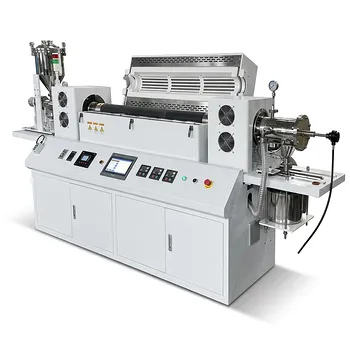
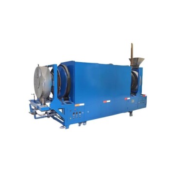
RF PECVD System Radio Frequency Plasma-Enhanced Chemical Vapor Deposition

RF PECVD System Radio Frequency Plasma-Enhanced Chemical Vapor Deposition

RF-PECVD is an acronym for "Radio Frequency Plasma-Enhanced Chemical Vapor Deposition." It deposits DLC (Diamond-like carbon film) on germanium and silicon substrates. It is utilized in the 3-12um infrared wavelength range.
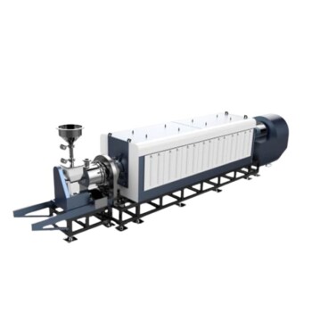
Slide PECVD tube furnace with liquid gasifier PECVD machine

Slide PECVD tube furnace with liquid gasifier PECVD machine

KT-PE12 Slide PECVD System: Wide power range, programmable temp control, fast heating/cooling with sliding system, MFC mass flow control & vacuum pump.

Electron Beam Evaporation Coating Oxygen-Free Copper Crucible

Electron Beam Evaporation Coating Oxygen-Free Copper Crucible

Electron Beam Evaporation Coating Oxygen-Free Copper Crucible enables precise co-deposition of various materials. Its controlled temperature and water-cooled design ensure pure and efficient thin film deposition.

Cylindrical Resonator MPCVD Diamond Machine for lab diamond growth

Cylindrical Resonator MPCVD Diamond Machine for lab diamond growth

Learn about Cylindrical Resonator MPCVD Machine, the microwave plasma chemical vapor deposition method used for growing diamond gemstones and films in the jewelry and semi-conductor industries. Discover its cost-effective advantages over traditional HPHT methods.

Bell-jar Resonator MPCVD Diamond Machine for lab and diamond growth

Bell-jar Resonator MPCVD Diamond Machine for lab and diamond growth

Get high-quality diamond films with our Bell-jar Resonator MPCVD machine designed for lab and diamond growth. Discover how Microwave Plasma Chemical Vapor Deposition works for growing diamonds using carbon gas and plasma.

CVD diamond for thermal management

CVD diamond for thermal management

CVD diamond for thermal management: High-quality diamond with thermal conductivity up to 2000 W/mK, ideal for heat spreaders, laser diodes, and GaN on Diamond (GOD) applications.

Ceramic Evaporation Boat Set

Ceramic Evaporation Boat Set

It can be used for vapor deposition of various metals and alloys. Most metals can be evaporated completely without loss. Evaporation baskets are reusable.1

Hemispherical Bottom Tungsten / Molybdenum Evaporation Boat

Hemispherical Bottom Tungsten / Molybdenum Evaporation Boat

Used for gold plating, silver plating, platinum, palladium, suitable for a small amount of thin film materials. Reduce the waste of film materials and reduce heat dissipation.

CVD boron doped diamond

CVD boron doped diamond

CVD boron-doped diamond: A versatile material enabling tailored electrical conductivity, optical transparency, and exceptional thermal properties for applications in electronics, optics, sensing, and quantum technologies.

915MHz MPCVD Diamond Machine

915MHz MPCVD Diamond Machine

915MHz MPCVD Diamond Machine and its multi-crystal effective growth, the maximum area can reach 8 inches, the maximum effective growth area of single crystal can reach 5 inches. This equipment is mainly used for the production of large-size polycrystalline diamond films, the growth of long single crystal diamonds, the low-temperature growth of high-quality graphene, and other materials that require energy provided by microwave plasma for growth.

Aluminized ceramic evaporation boat

Aluminized ceramic evaporation boat

Vessel for depositing thin films; has an aluminum-coated ceramic body for improved thermal efficiency and chemical resistance. making it suitable for various applications.

Customer made versatile CVD tube furnace CVD machine

Customer made versatile CVD tube furnace CVD machine

Get your exclusive CVD furnace with KT-CTF16 Customer Made Versatile Furnace. Customizable sliding, rotating, and tilting functions for precise reactions. Order now!

High Purity Palladium (Pd) Sputtering Target / Powder / Wire / Block / Granule

High Purity Palladium (Pd) Sputtering Target / Powder / Wire / Block / Granule

Looking for affordable Palladium materials for your lab? We offer custom solutions with varying purities, shapes, and sizes - from sputtering targets to nanometer powders and 3D printing powders. Browse our range now!

High Purity Vanadium (V) Sputtering Target / Powder / Wire / Block / Granule

High Purity Vanadium (V) Sputtering Target / Powder / Wire / Block / Granule

Looking for high-quality Vanadium (V) materials for your laboratory? We offer a wide range of customizable options to fit your unique needs, including sputtering targets, powders, and more. Contact us today for competitive pricing.

CVD Diamond coating

CVD Diamond coating

CVD Diamond Coating: Superior Thermal Conductivity, Crystal Quality, and Adhesion for Cutting Tools, Friction, and Acoustic Applications

Optical Windows

Optical Windows

Diamond optical windows: exceptional broad band infrared transparency, excellent thermal conductivity & low scattering in infrared, for high-power IR laser & microwave windows applications.

Platinum disc electrode

Platinum disc electrode

Upgrade your electrochemical experiments with our Platinum Disc Electrode. High-quality and reliable for accurate results.

PTFE conductive glass substrate cleaning rack

PTFE conductive glass substrate cleaning rack

The PTFE conductive glass substrate cleaning rack is used as the carrier of the square solar cell silicon wafer to ensure efficient and pollution-free handling during the cleaning process.

Drawing die nano-diamond coating HFCVD Equipment

Drawing die nano-diamond coating HFCVD Equipment

The nano-diamond composite coating drawing die uses cemented carbide (WC-Co) as the substrate, and uses the chemical vapor phase method ( CVD method for short ) to coat the conventional diamond and nano-diamond composite coating on the surface of the inner hole of the mold.

Related Articles

Plasma Enhanced Chemical Vapor Deposition (PECVD): A Comprehensive Guide

Plasma Enhanced Chemical Vapor Deposition (PECVD): A Comprehensive Guide

Learn everything you need to know about Plasma Enhanced Chemical Vapor Deposition (PECVD), a thin film deposition technique used in the semiconductor industry. Explore its principles, applications, and benefits.

Find out more
Understanding PECVD: A Guide to Plasma-Enhanced Chemical Vapor Deposition

Understanding PECVD: A Guide to Plasma-Enhanced Chemical Vapor Deposition

PECVD is a useful technique for creating thin film coatings because it allows for the deposition of a wide variety of materials, including oxides, nitrides, and carbides.

Find out more
The Role of Plasma in PECVD Coatings

The Role of Plasma in PECVD Coatings

PECVD (Plasma Enhanced Chemical Vapor Deposition) is a type of thin film deposition process that is widely used for creating coatings on various substrates. In this process, a plasma is used to deposit thin films of various materials onto a substrate.

Find out more
An Introduction to Chemical Vapor Deposition (CVD)

An Introduction to Chemical Vapor Deposition (CVD)

Chemical vapor deposition, or CVD, is a coating process that involves the use of gaseous reactants to produce thin films and coatings of high quality.

Find out more
Advantages and Disadvantages of Chemical Vapor Deposition (CVD)

Advantages and Disadvantages of Chemical Vapor Deposition (CVD)

Chemical vapor deposition (CVD) is a versatile thin-film deposition technique widely used in various industries. Explore its advantages, disadvantages, and potential new applications.

Find out more
Comparing the Performance of PECVD and HPCVD in Coating Applications

Comparing the Performance of PECVD and HPCVD in Coating Applications

Although both PECVD & HFCVD are used for coating applications, they differ in terms of deposition methods, performance, and suitability for specific applications.

Find out more
CVD Machines for Thin Film Deposition

CVD Machines for Thin Film Deposition

Chemical Vapor Deposition (CVD) is a widely used technique for deposition of thin films on various substrates.

Find out more
Why PECVD is Essential for Microelectronic Device Fabrication

Why PECVD is Essential for Microelectronic Device Fabrication

PECVD (Plasma-Enhanced Chemical Vapor Deposition) is a popular thin film deposition technique used in microelectronics device fabrication.

Find out more
A Step-by-Step Guide to the PECVD Process

A Step-by-Step Guide to the PECVD Process

PECVD is a type of chemical vapor deposition process that uses plasma to enhance the chemical reactions between the gas-phase precursors and the substrate.

Find out more
A Comprehensive Guide to PECVD Equipment Maintenance

A Comprehensive Guide to PECVD Equipment Maintenance

Proper maintenance of PECVD equipment is crucial to ensure its optimal performance, longevity, and safety.

Find out more
Comparing Chemical Vapor Deposition and Physical Vapor Deposition

Comparing Chemical Vapor Deposition and Physical Vapor Deposition

Chemical Vapor Deposition (CVD) VS Physical Vapor Deposition (PVD)

Find out more
The Process of Fabricating a CVD Diamond By MPCVD Machine

The Process of Fabricating a CVD Diamond By MPCVD Machine

CVD diamond machines have gained significant importance in various industries and scientific research.

Find out more