Chemical Vapor Deposition (CVD)
Chemical vapor deposition (CVD) is a process used to produce thin films of materials by the decomposition of a gas or vapor onto a substrate. In CVD, a precursor, which is a gas or vapor containing the desired chemical elements, is introduced into a reaction chamber.
The precursor molecules are then decomposed and react on the surface of the substrate to form the desired thin film. The flow of the precursor and other process parameters, such as temperature and pressure, are carefully controlled to ensure a consistent and high-quality thin film.
CVD is often used to deposit a wide range of materials, including metals, semiconductors, ceramics, and polymers.
Physical Vapor Deposition (PVD)
Physical vapor deposition (PVD) is a process used to produce thin films of materials by the condensation of a vaporized form of the material onto a substrate. PVD involves the vaporization of a solid material, which can be done by several methods such as evaporation, sputtering, or molecular beam epitaxy (MBE).
PVD is often used to deposit a wide range of materials, including metals, semiconductors, and insulators. It is known for producing high-quality, uniform thin films with excellent structural and electrical properties.
- In evaporation, the material to be deposited is heated until it vaporizes and then transported to the substrate where it condenses to form a thin film. This process can be done using a resistive heating method, in which the material is placed in a crucible and heated by passing an electric current through it, or using a beam heating method, in which the material is bombarded with a high-energy beam, such as a laser, to vaporize it.
- In sputtering, a solid target material is bombarded with high-energy ions, which cause atoms of the material to be sputtered off the target and deposited onto the substrate as a thin film. A plasma, which is a gas containing ions and electrons, is generated in the process chamber, and a voltage is applied between the target and the substrate to accelerate the ions towards the target. When the ions strike the target, they cause atoms of the material to be sputtered off and deposited onto the substrate.
- In molecular beam epitaxy (MBE), a beam of atoms or molecules is directed onto the substrate, where they react and condense to form a thin film. The substrate is first cleaned and loaded into a vacuum chamber, which is evacuated and heated to drive off surface contaminants and roughen the surface of the substrate. The molecular beams are then emitted through a shutter, and the desired material collects on the substrate as a thin film. MBE is known for producing high-quality, highly uniform thin films with excellent structural and electrical properties.
Advantages and Disadvantages
Temperature
One of the main differences between chemical vapor deposition (CVD) and physical vapor deposition (PVD) is the temperature required for the process. CVD processes typically run at higher temperatures, usually between 300°C and 900°C, while PVD processes can run at lower temperatures, often below 200°C. This difference in temperature requirement can be a factor in choosing between the two processes, as it can influence the properties of the thin film and the compatibility with the substrate material.
CVD processes often require high temperatures in order to drive the chemical reactions that occur during the thin film formation. The heat can be supplied by a furnace, RF coil, or laser, and it is used to heat the precursor gases and the substrate to the desired temperature. The high temperature can lead to higher waste deposition and can also cause thermal stress on the substrate, which may limit its use for certain materials. However, the high temperature also allows for the formation of high-quality thin films with good structural and electrical properties.
On the other hand, PVD processes typically operate at lower temperatures and do not involve chemical reactions. The material is vaporized by methods such as evaporation, sputtering, or MBE and then condensed onto the substrate to form a thin film. The lower temperature of PVD processes makes them more suitable for substrate materials that cannot withstand high temperatures, such as plastics and certain ceramics. However, the lower temperature can also lead to the formation of less dense and less well-adhered thin films compared to CVD.
Laser-assisted chemical vapor deposition (LCVD) is a variant of chemical vapor deposition (CVD) that uses a laser to heat the substrate and the precursor gases to the desired temperature. In LCVD, the laser beam is focused onto the substrate, and the energy from the laser is absorbed by the substrate, which heats it up. The precursor gases are then introduced into the reaction chamber and are decomposed and deposited on the surface of the substrate to form the thin film.
One advantage of LCVD over other CVD methods is that the laser beam can be moved over the substrate to selectively deposit the thin film in a specific pattern. This allows for the creation of complex and highly-patterned thin films, which can be difficult to achieve with other CVD methods. LCVD is also capable of producing high-quality thin films with excellent structural and electrical properties.
Molecular beam epitaxy (MBE), on the other hand, is a physical vapor deposition (PVD) method that allows for atomic-level control of the chemical composition, film thickness, and transition sharpness of the thin film. In MBE, a beam of atoms or molecules is directed onto the substrate, where they react and condense to form a thin film. The beam can be modulated to control the composition and thickness of the film, and the substrate temperature can be carefully controlled to achieve sharp transitions between different layers. MBE is known for producing high-quality, highly uniform thin films with excellent structural and electrical properties, but it is also a relatively expensive process. It is often used for applications that require high precision and control over the properties of the thin film.
Range of materials & safety
Sputtering is a physical vapor deposition (PVD) method that does not require the use of specialized precursor materials as in chemical vapor deposition (CVD). In sputtering, a solid target material is bombarded with high-energy ions, which cause atoms of the material to be sputtered off the target and deposited onto the substrate as a thin film. The target material can be a wide range of materials, including metals, alloys, and semiconductors, which makes sputtering a flexible and widely-used PVD method.
One advantage of PVD over CVD is the safety issue of the materials used in the process. Some precursors and by-products of CVD processes can be toxic, pyrophoric, or corrosive, which can cause issues with material handling and storage. PVD processes, on the other hand, do not involve chemical reactions and do not produce hazardous by-products, which makes them safer to use and easier to handle.
There are many factors to consider when choosing between CVD and PVD for a particular application. An experienced engineer can evaluate the cost, film thickness, source material availability, compositional control, and other criteria to recommend the most suitable deposition method. Both CVD and PVD have their own advantages and limitations, and the choice of the method depends on the specific requirements of the application.
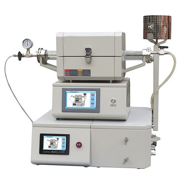
Kindle Tech Lab CVD Furnace
I recommend the Kindle Tech CVD furnace for those in need of a high-quality, reliable furnace for chemical vapor deposition (CVD) processes. This furnace is designed specifically for CVD applications and features a range of advanced features to ensure consistent and repeatable results. The furnace is equipped with precision temperature control and a powerful heating element, which allows for fast ramp-up and cool-down times and precise temperature control. The reaction chamber is spacious and can accommodate a wide range of substrates, and the furnace is easy to operate with a user-friendly interface.
Customize CVD furnace according to your needs
Kindle Tech is a company that specializes in the design and manufacture of furnaces for chemical vapor deposition (CVD) processes. The company offers a range of standard CVD furnace models, but they also have the capability to customize furnaces to meet the specific needs and requirements of their customers.
Customization options for Kindle Tech CVD furnaces include various chamber sizes and shapes, multiple heating options, custom gas delivery systems, and a range of additional features and accessories. The company has a team of experienced engineers who can work with customers to design and build a custom CVD furnace that meets their specific requirements.
If you are in need of a CVD furnace with specific features or capabilities that are not available in standard models, Kindle Tech may be able to provide a custom solution. You can contact us to discuss your specific needs and get more information on the customization options available.
Related Products
- Chemical Vapor Deposition CVD Equipment System Chamber Slide PECVD Tube Furnace with Liquid Gasifier PECVD Machine
- Microwave Plasma Chemical Vapor Deposition MPCVD Machine System Reactor for Lab and Diamond Growth
- 915MHz MPCVD Diamond Machine Microwave Plasma Chemical Vapor Deposition System Reactor
- Customer Made Versatile CVD Tube Furnace Chemical Vapor Deposition Chamber System Equipment
- HFCVD Machine System Equipment for Drawing Die Nano-Diamond Coating
Related Articles
- PECVD Furnace A Low-Power and Low-Temperature Solution for Soft Matter
- A Comprehensive Guide to PECVD Equipment Maintenance
- In-Depth Examination of Chemical Vapor Deposition (CVD) Coatings
- Advantages of Chemical Vapor Deposition
- Advantages, Limitations, and Process Control of Chemical Vapor Deposition (CVD) Technology


