CVD materials
Laboratory CVD Boron Doped Diamond Materials
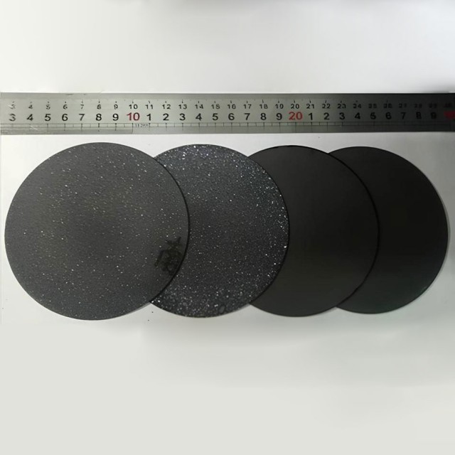
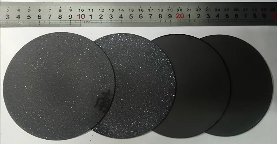
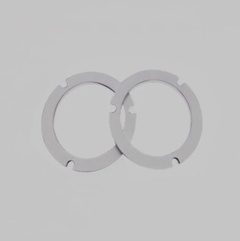
Item Number : cvdm-07
Price varies based on specs and customizations
- Diameter
- 100mm
- thickness
- 0.3-2mm
Shipping:
Contact us to get shipping details Enjoy On-time Dispatch Guarantee.
Why Choose Us
Easy ordering process, quality products, and dedicated support for your business success.
Introduction
Chemical Vapor Deposition (CVD) boron-doped diamond is a unique material that combines the extraordinary properties of diamond with controllable electrical conductivity. By precisely introducing boron atoms into the diamond lattice during CVD growth, it becomes a versatile material with tailored electrical properties, ranging from insulating to highly conductive. This enables diverse applications in electronics, sensors, heat management, optics, and quantum technologies.
Applications
Chemical Vapor Deposition (CVD) boron-doped diamond is a versatile material with exceptional properties, offering unique solutions to challenges across multiple industries, from electronics to quantum technologies. Its continued development and integration into various applications hold great promise for advancing technology and scientific research in the years to come.
- Electronics: High-power electronic devices, high-frequency transistors, diodes, field-effect transistors (FETs)
- Sensors: Temperature, pressure, radiation, gas composition
- Heat Management: Heat spreaders, heat sinks, thermal management solutions
- Optics and Photonics: Optical windows, lenses, substrate for quantum optics experiments
- Quantum Technologies: Quantum computing, quantum communication, quantum sensing applications
Features
-
Exceptional Thermal Conductivity: CVD boron-doped diamond possesses outstanding thermal conductivity, enabling efficient dissipation of heat in high-power electronics, laser systems, and microelectronics.
-
Tailorable Electrical Conductivity: Through precise control of boron concentration during the CVD growth process, the electrical conductivity of CVD boron-doped diamond can be customized over a wide range, from insulating to highly conductive.
-
Broad Spectral Transparency: CVD boron-doped diamond exhibits transparency across a broad spectral range, making it suitable for applications in optics and photonics, such as optical windows and lenses.
-
Color Center Hosting: Boron-doped diamond can host color centers, which are defects in the diamond lattice that exhibit unique optical properties. These color centers have applications in quantum optics experiments and quantum information processing.
-
High Breakdown Voltage: CVD boron-doped diamond can withstand high breakdown voltages, making it ideal for high-power electronic devices operating in harsh environments.
-
High Carrier Mobility: Boron-doped diamond possesses high carrier mobility, enabling faster switching speeds and improved performance in electronic devices.
-
Wide Potential Window: Boron-doped diamond has a wide potential window of approximately 3.5 V, allowing for the application of "over-potentials" to stimulate high-energy chemical reactions.
-
Low Background Currents: Boron-doped diamond electrodes exhibit low background currents in cyclic voltammetry scans due to the small capacitance-layer at the semiconductor-like interface with electrolyte solutions.
-
Chemical Inertness: CVD boron-doped diamond is chemically inert, making it resistant to corrosion and suitable for harsh environments.
-
Quantum Properties: Boron-doped diamond has promising applications in quantum technologies, such as quantum computing, quantum communication, and quantum sensing, due to its long coherence times and ability to host individual quantum bits (qubits) at room temperature.
Principle
Chemical Vapor Deposition (CVD) boron-doped diamond is created by introducing boron atoms into the diamond lattice during the CVD growth process. This doping process controls the material's electrical conductivity, allowing for customization from insulating to highly conductive.
Advantages
-
Semiconducting Behavior: Boron doping introduces charge carriers into the diamond lattice, enabling control of electrical conductivity, ranging from insulating to highly conductive, making it suitable for various electronic applications.
-
High Thermal Conductivity: Boron-doped diamond possesses exceptional thermal conductivity, surpassing other semiconductors, enabling efficient heat dissipation in high-power electronic devices, laser systems, and microelectronics.
-
Wide Spectral Transparency: Boron-doped diamond exhibits transparency across a broad spectral range, from ultraviolet to infrared, making it valuable for optical windows, lenses, and applications in optics and photonics.
-
Color Centers: Boron-doped diamond can host color centers, which are atomic-scale defects with unique optical and spin properties. These color centers find applications in quantum technologies, including quantum computing, quantum communication, and quantum sensing.
-
Chemical Inertness: Boron-doped diamond is chemically inert, resistant to harsh environments, and compatible with various chemicals, making it suitable for applications in corrosive or extreme conditions.
-
Mechanical Hardness: Boron-doped diamond inherits the exceptional mechanical hardness of diamond, providing durability and resistance to wear and tear, even in demanding applications.
-
Tailored Electrical Properties: The concentration of boron atoms can be precisely controlled during the CVD growth process, allowing for customization of the material's electrical conductivity over a wide range, enabling optimization for specific applications.
-
Low Temperature Deposition: Chemical Vapor Deposition (CVD) process is typically carried out at low temperatures, enabling integration with a wide range of substrates and compatibility with various device fabrication processes.
-
Industrial Compatibility: CVD boron-doped diamond is compatible with industrial manufacturing processes, enabling scalable and cost-effective production, making it suitable for high-volume applications.
Specification
| Available dimension: | Diameter100mm, thickness 0.3-2mm |
|---|---|
| Boron Concentration [B]: | 2 to 6 x 10²⁰ Atoms /cm3, averaged over 0.16 mm2 |
| Bulk Resistivity (Rv): | 2 to 1.8 x 10⁻³ Ohm m, ± 0.25 x 10⁻³ Ohm m |
| Solvent Window: | >3.0V |
Trusted by Industry Leaders
FAQ
What Are The Main Applications Of Diamond Materials?
What Are The Key Advantages And Applications Of Chemical Vapor Deposition (CVD) Boron-doped Diamond?
What Are The Advantages Of Using Diamond Materials In Industrial Applications?
What Is CVD Diamond Machine?
How Is Boron Doping Achieved During The Growth Of Diamond Films?
What Types Of Diamond Materials Are Available?
How Does A CVD Diamond Machine Work?
What Is The Relationship Between The Concentration Of Boron Atoms And The Electrical Conductivity Of The Diamond Film?
What Is The Principle Behind The Use Of Diamond Materials In Cutting Tools?
What Are The Advantages Of Using CVD Diamond Machines?
How Can The Electrical Conductivity Of The Diamond Film Be Tailored?
Why Is Synthetic Diamond Preferred Over Natural Diamond In Industrial Applications?
What Considerations Should Be Made When Selecting A CVD Diamond Machine?
What Are The Limitations Or Challenges Associated With The Fabrication Of Boron-doped Diamond Films?
What Are The Common Applications Of Diamonds Produced By CVD Diamond Machines?
REQUEST A QUOTE
Our professional team will reply to you within one business day. Please feel free to contact us!
Related Products

CVD Diamond for Thermal Management Applications
CVD diamond for thermal management: High-quality diamond with thermal conductivity up to 2000 W/mK, ideal for heat spreaders, laser diodes, and GaN on Diamond (GOD) applications.

Custom CVD Diamond Coating for Lab Applications
CVD Diamond Coating: Superior Thermal Conductivity, Crystal Quality, and Adhesion for Cutting Tools, Friction, and Acoustic Applications

CVD Diamond Domes for Industrial and Scientific Applications
Discover CVD diamond domes, the ultimate solution for high-performance loudspeakers. Made with DC Arc Plasma Jet technology, these domes deliver exceptional sound quality, durability, and power handling.

CVD Diamond Dressing Tools for Precision Applications
Experience the Unbeatable Performance of CVD Diamond Dresser Blanks: High Thermal Conductivity, Exceptional Wear Resistance, and Orientation Independence.

915MHz MPCVD Diamond Machine Microwave Plasma Chemical Vapor Deposition System Reactor
915MHz MPCVD Diamond Machine and its multi-crystal effective growth, the maximum area can reach 8 inches, the maximum effective growth area of single crystal can reach 5 inches. This equipment is mainly used for the production of large-size polycrystalline diamond films, the growth of long single crystal diamonds, the low-temperature growth of high-quality graphene, and other materials that require energy provided by microwave plasma for growth.

CVD Diamond Optical Windows for Lab Applications
Diamond optical windows: exceptional broad band infrared transparency, excellent thermal conductivity & low scattering in infrared, for high-power IR laser & microwave windows applications.

CVD Diamond Cutting Tool Blanks for Precision Machining
CVD Diamond Cutting Tools: Superior Wear Resistance, Low Friction, High Thermal Conductivity for Non-Ferrous Materials, Ceramics, Composites Machining

Microwave Plasma Chemical Vapor Deposition MPCVD Machine System Reactor for Lab and Diamond Growth
Get high-quality diamond films with our Bell-jar Resonator MPCVD machine designed for lab and diamond growth. Discover how Microwave Plasma Chemical Vapor Deposition works for growing diamonds using carbon gas and plasma.

HFCVD Machine System Equipment for Drawing Die Nano-Diamond Coating
The nano-diamond composite coating drawing die uses cemented carbide (WC-Co) as the substrate, and uses the chemical vapor phase method ( CVD method for short ) to coat the conventional diamond and nano-diamond composite coating on the surface of the inner hole of the mold.

CVD Diamond Wire Drawing Die Blanks for Precision Applications
CVD diamond wire drawing die blanks: superior hardness, abrasion resistance, and applicability in wire drawing various materials. Ideal for abrasive wear machining applications like graphite processing.

Cylindrical Resonator MPCVD Machine System Reactor for Microwave Plasma Chemical Vapor Deposition and Lab Diamond Growth
Learn about Cylindrical Resonator MPCVD Machine, the microwave plasma chemical vapor deposition method used for growing diamond gemstones and films in the jewelry and semi-conductor industries. Discover its cost-effective advantages over traditional HPHT methods.

Electron Beam Evaporation Coating Conductive Boron Nitride Crucible BN Crucible
High-purity and smooth conductive boron nitride crucible for electron beam evaporation coating, with high temperature and thermal cycling performance.
Conductive Boron Nitride BN Ceramics Composite for Advanced Applications
Due to the characteristics of boron nitride itself, the dielectric constant and dielectric loss are very small, so it is an ideal electrical insulating material.
Hexagonal Boron Nitride HBN Ceramic Ring
Boron nitride ceramic (BN) rings are commonly used in high temperature applications such as furnace fixtures, heat exchangers and semiconductor processing.

Boron Nitride (BN) Ceramic Plate
Boron nitride (BN) ceramic plates do not use aluminum water to wet, and can provide comprehensive protection for the surface of materials that directly contact molten aluminum, magnesium, zinc alloys and their slag.

Customer Made Versatile CVD Tube Furnace Chemical Vapor Deposition Chamber System Equipment
Get your exclusive CVD furnace with KT-CTF16 Customer Made Versatile Furnace. Customizable sliding, rotating, and tilting functions for precise reactions. Order now!

RF PECVD System Radio Frequency Plasma-Enhanced Chemical Vapor Deposition RF PECVD
RF-PECVD is an acronym for "Radio Frequency Plasma-Enhanced Chemical Vapor Deposition." It deposits DLC (Diamond-like carbon film) on germanium and silicon substrates. It is utilized in the 3-12um infrared wavelength range.
Boron Nitride (BN) Ceramic Rod for High Temperature Applications
Boron nitride (BN) rod is the strongest boron nitride crystal form like graphite, which has excellent electrical insulation, chemical stability and dielectric properties.
Boron Nitride (BN) Ceramic Tube
Boron nitride (BN) is known for its high thermal stability, excellent electrical insulating properties and lubricating properties.
Custom Boron Nitride (BN) Ceramic Parts
Boron nitride (BN) ceramics can have different shapes, so they can be manufactured to generate high temperature, high pressure, insulation and heat dissipation to avoid neutron radiation.
Related Articles

How to Check if Your Diamond is CVD-Produced
When it comes to buying a diamond, it's important to understand the difference between a naturally occurring diamond and one produced using CVD technology.
Market Prospects and Applications of CVD Diamonds
Explores the unique properties of CVD diamonds, their preparation methods, and diverse applications in various fields.
CVD Diamond: Superior Material for Optical Windows
Explores the exceptional properties and applications of CVD diamond in optical windows.
Preparation and Transfer Technology of Graphene by Chemical Vapor Deposition
This article reviews the preparation methods of graphene, with a focus on CVD technology, its transfer techniques, and future prospects.
An Introduction to Chemical Vapor Deposition (CVD)
Chemical vapor deposition, or CVD, is a coating process that involves the use of gaseous reactants to produce thin films and coatings of high quality.
Chemical Vapor Deposition (CVD) of Graphene Challenges and Solutions
Chemical Vapor Deposition (CVD) is a widely adopted method for the production of high-quality graphene.
Advantages and Disadvantages of Chemical Vapor Deposition (CVD)
Chemical vapor deposition (CVD) is a versatile thin-film deposition technique widely used in various industries. Explore its advantages, disadvantages, and potential new applications.
Coating Methods for Growing Single Crystal Films
An overview of various coating methods like CVD, PVD, and Epitaxy for growing single crystal films.
CVD Machines for Thin Film Deposition
Chemical Vapor Deposition (CVD) is a widely used technique for deposition of thin films on various substrates.
Technical Overview of Silicon-Carbon Anode Materials Prepared by CVD Method
This article discusses the key technical aspects of silicon-carbon anode materials prepared via CVD, focusing on their synthesis, performance improvements, and industrial application potential.
How CVD is Used in the Semiconductor Industry
CVD has revolutionized the semiconductor industry, enabling the production of high-performance electronic devices with enhanced functionality and reliability.
Comprehensive Overview of Chemical Vapor Deposition (CVD) Technologies
This article details various CVD technologies used in semiconductor and thin film deposition industries.