Introduction to PECVD
PECVD (Plasma-Enhanced Chemical Vapor Deposition) is a popular thin film deposition technique used in microelectronics device fabrication. It is a low-temperature process that involves depositing a thin film of a material onto a substrate using plasma. The process involves introducing a gas into a vacuum chamber, which is then excited by a plasma source. The excited gas molecules react with the substrate surface, forming a thin film. PECVD is widely used because it offers several advantages over other deposition techniques, including high deposition rates, low-temperature processing, and excellent film uniformity.
Table of Contents
Advantages of PECVD over other deposition techniques
PECVD offers several advantages over other deposition techniques like physical vapor deposition (PVD) and chemical vapor deposition (CVD). Here are the key advantages of PECVD:
Ability to deposit a wider range of materials
PECVD can deposit a wider range of materials than other deposition techniques. It can be used to deposit various materials, including silicon dioxide, silicon nitride, and amorphous silicon on a variety of substrates such as metals, glass, and plastics.
Excellent film uniformity
PECVD can produce films with a uniform thickness and excellent adhesion to the substrate. The broad range of control of plasma-chemical reactions and plasma-surface interactions allows one to optimize the film composition and microstructure. The films generally possess a high packing density, which makes them hard and environmentally stable.
Low-temperature processing
PECVD operates at low temperatures, making it suitable for heat-sensitive substrates. The absence of abrupt interfaces leads to a uniform distribution or compensation of internal stresses, generally giving rise to enhanced adhesion and mechanical integrity.
High scalability
PECVD is a highly scalable process, making it ideal for large-scale manufacturing. Different substrate shapes, including 3D, can be uniformly coated, making it suitable for a wide range of applications, including the deposition of thin films for microelectronic devices, photovoltaic cells, and display panels.
In summary, PECVD offers a wide range of advantages over other deposition techniques, including the ability to deposit a wider range of materials, excellent film uniformity, low-temperature processing, high throughput, and high scalability. These unique advantages make PECVD an indispensable tool for the semiconductor industry, enabling the production of high-quality microelectronic devices that power our modern world.
Applications of PECVD in Different Industries
Semiconductor Industry
PECVD is widely used in the semiconductor industry to deposit thin films of silicon dioxide and silicon nitride, which are used as insulators and passivation layers in microelectronic devices. These materials are essential for isolating multiple conductive layers and capacitors in microelectronic devices. PECVD is also used in the production of thin-film transistors (TFTs) for displays and other electronic devices. TFTs are an essential component of modern displays, and PECVD is a key technology for their fabrication.
Solar Industry
PECVD is used to deposit thin films of amorphous silicon in the manufacture of thin-film solar cells. Thin-film solar cells are lightweight, flexible, and can be produced in large areas, making them ideal for many applications, including in portable electronic devices and building-integrated photovoltaics (BIPV). PECVD is also used to deposit anti-reflective coatings on solar panels, which helps to improve their efficiency.
Display Industry
In the display industry, PECVD is used to deposit thin films of silicon dioxide and silicon nitride as encapsulation layers in organic light-emitting diodes (OLEDs) and thin-film transistors (TFTs). These materials play a crucial role in protecting the OLEDs and TFTs from moisture and oxygen, which can degrade their performance and reduce their lifespan. PECVD is also used to deposit transparent conductive oxides (TCOs) in the manufacture of touchscreens, which are used in a wide range of electronic devices.
Other Industries
PECVD has a range of other applications in various industries, including the biomedical industry, where it is used to deposit biocompatible coatings on medical implants. PECVD is also used in the food packaging industry to produce very dense, inert coatings with an extremely high degree of purity. These coatings help to extend the shelf life of the food and protect it from contamination.
In conclusion, PECVD is an essential technique for the fabrication of microelectronic devices and has applications in a wide range of industries. Its versatility and effectiveness make it an invaluable tool for the manufacture of various electronic devices, solar panels, touchscreens, and medical implants. PECVD is a highly efficient technique that allows for the deposition of high-quality films at low temperatures, which is essential for the manufacture of microelectronic devices.
Common PECVD Applications in Microelectronics
PECVD is a crucial technology in the microelectronics industry and offers significant advantages in terms of efficiency, quality, and cost-effectiveness. Here are some of the most common PECVD applications in microelectronics:
Silicon dioxide deposition
PECVD is widely used in the manufacturing of microelectronic devices such as integrated circuits, flat panel displays, and solar cells. The technique is highly effective in depositing materials such as silicon dioxide, which is essential for the functioning of electronic devices. Silicon dioxide is used as an insulator in electronic devices and is deposited by PECVD at a low temperature, making it ideal for use in the manufacturing of microelectronic devices.
Silicon nitride deposition
Another important application of PECVD in microelectronics is the deposition of silicon nitride. Silicon nitride is deposited by PECVD at a low temperature and is widely used in the creation of anti-reflective coatings, passivation layers, and barrier coatings. The process is ideal for creating uniform, high-quality films with precise thickness and excellent adhesion properties.
Amorphous silicon deposition
PECVD is also used in the deposition of amorphous silicon, which is essential for the functioning of electronic devices such as thin-film transistors and solar cells. The technique is highly effective in depositing amorphous silicon at a low temperature, making it ideal for use in the manufacturing of microelectronic devices.
Anti-reflective coatings
PECVD is widely used in the creation of anti-reflective coatings. These coatings are used in microelectronic devices such as flat panel displays and solar cells to reduce reflection and improve efficiency. PECVD is ideal for creating uniform, high-quality films with precise thickness and excellent adhesion properties.
Passivation layers
PECVD is also used in the creation of passivation layers, which are used to protect the surface of microelectronic devices from external influences such as moisture, dust, and other contaminants. Passivation layers are deposited by PECVD at a low temperature, making it ideal for use in the manufacturing of microelectronic devices.
In conclusion, PECVD is a versatile technique that can be used to deposit thin films on a wide range of materials, including glass, metals, and ceramics. Its applications in the microelectronics industry are numerous, and it is highly effective in depositing materials such as silicon dioxide, silicon nitride, and amorphous silicon, which are essential for the functioning of electronic devices. PECVD offers significant advantages in terms of efficiency, quality, and cost-effectiveness, making it an essential technology in the microelectronics industry.
Conclusion on PECVD's importance in microelectronics
PECVD is an essential technique for fabricating microelectronic devices due to its ability to deposit high-quality thin films onto substrates. It offers several advantages over other deposition techniques, including its low-temperature process, high rate of deposition, and excellent uniformity of films. PECVD finds applications in various industries, including microelectronics, solar cells, and optical coatings. The PECVD systems market is growing due to the increasing demand for microelectronic devices and the need for better-quality thin films. In conclusion, PECVD is an important technology in microelectronics, and its usage is expected to grow further in the future.
Related Products
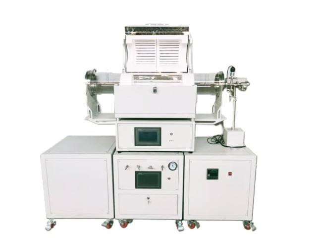
- Chemical Vapor Deposition CVD Equipment System Chamber Slide PECVD Tube Furnace with Liquid Gasifier PECVD Machine
- RF PECVD System Radio Frequency Plasma-Enhanced Chemical Vapor Deposition RF PECVD
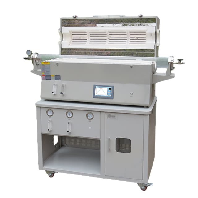
- Inclined Rotary Plasma Enhanced Chemical Vapor Deposition PECVD Equipment Tube Furnace Machine
- Inclined Rotary Plasma Enhanced Chemical Vapor Deposition PECVD Equipment Tube Furnace Machine
- 915MHz MPCVD Diamond Machine Microwave Plasma Chemical Vapor Deposition System Reactor
Related Articles
- Understanding the PECVD Method
- Comprehensive Overview of 12 Types of Chemical Vapor Deposition (CVD) Techniques
- Comparing Chemical Vapor Deposition and Physical Vapor Deposition
- In-Depth Examination of Chemical Vapor Deposition (CVD) Coatings
- Detailed Processes and Parameters of PECVD for TiN and Si3N4 Deposition


