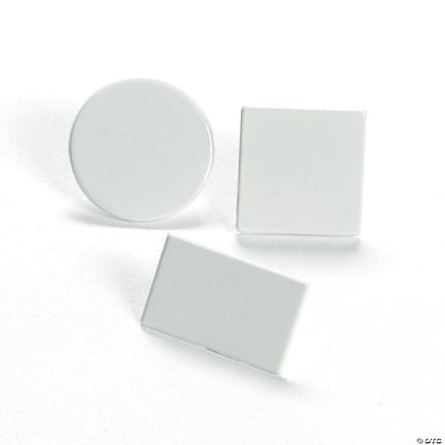
Optical Materials
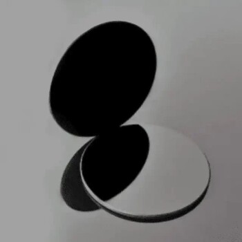
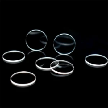
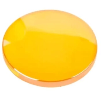
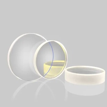
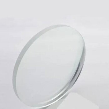
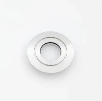
Infrared High Resistance Single Crystal Silicon Lens
Item Number : KTOM-HBS
Price varies based on specs and customizations
- Diameter
- +0/-0.2mm
- Thickness
- +/-0.1mm
- Surface Quality
- 60/40
Shipping:
Contact us to get shipping details Enjoy On-time Dispatch Guarantee.
Why Choose Us
Easy ordering process, quality products, and dedicated support for your business success.
Single Crystal Silicon
Single Crystal Silicon exhibits a transmission range of 1.2 to 8 microns (uncoated). However, it demonstrates a strong absorption band at 9 microns, making it particularly suitable for applications within the 3-5 micron range. Beyond this, floating zone silicon can be utilized. This material offers numerous advantages, including its affordability, making it an excellent choice for weight-sensitive applications. Furthermore, monocrystalline silicon possesses a lower density, greater hardness, and improved durability compared to germanium, rendering it less prone to brittleness. Consequently, it finds extensive application in various industries such as the military, imaging, scientific research, as well as optical coating substrates.
Detail & Parts


Advantages of Silicon windows
- Silicon windows have a low density of 2.329 g/cm3, ideal for weight-sensitive applications. In addition, silicon is not as brittle as germanium and zinc selenide, and has better thermal stability.
- Since silicon has a cubic crystal structure, it does not exhibit birefringence. Birefringence degrades infrared imaging performance, so it is important to choose a non-birefringent material.
Specifications of silicate glass
| Material | Single crystal of Silicon(Si) |
| Crystal structure | Face-centred Cubic |
| Applicable wave band | 1.2μm ~ 8μm |
| Refractive index | 3.4223 @5 μm |
| Thermal conductivity | 273.3 W/mK |
| Coefficient of thermal expansion | 2.6×10⁻⁶/℃ at 20℃ |
Provide customized services
Through the implementation of innovative and state-of-the-art melting processes, we have acquired extensive expertise in the development and manufacture of quality glass products, offering a wide range of optical glass products for a variety of commercial, industrial and scientific applications. The company provides various specifications of optical glass such as raw glass, cut parts and finished components, and cooperates closely with customers to customize products according to customer needs. With an unwavering commitment to quality, we ensure our customers receive the perfect solution tailored to their requirements.
For further quotations, please contact us.
Trusted by Industry Leaders
FAQ
What Are The Main Types Of Glass Substrates?
What Does Silicon Do For Windows?
What Happens When Silicon Is Exposed To Air?
What Is The Difference Between Silicon And Glass?
What Is Optical Glass Used For?
What Is Soda-lime Glass Used For?
What Is The Composition Of Optical Glass?
What Are The Advantages Of Using Sapphire Substrates?
What Are The Most Common Optical Glasses?
Why Is Boroaluminosilicate Glass Suitable For Laboratory Glassware And Cooking Utensils?
What Are The Applications Of Optical Quartz Glass Sheets?
What Makes K9 Glass Special?
What Is A CaF2 Window Used For?
What Are The Properties Of Magnesium Fluoride Crystal Substrates?
What Is Silicon Used For In The Near-infrared Range?
What Are Glass Vibration Beads Used For In Laboratories?
REQUEST A QUOTE
Our professional team will reply to you within one business day. Please feel free to contact us!
Related Products
Infrared Thermal Imaging Temperature Measurement Double-Sided Coated Germanium Ge Lens
Germanium lenses are durable, corrosion-resistant optical lenses suited for harsh environments and applications exposed to the elements.
High Temperature Resistant Optical Quartz Glass Sheet
Discover the power of optical glass sheets for precise light manipulation in telecommunications, astronomy, and beyond. Unlock advancements in optical technology with exceptional clarity and tailored refractive properties.
Zinc Selenide ZnSe Optical Window Glass Substrate Wafer and Lens
Zinc selenide is formed by synthesizing zinc vapor with H2Se gas, resulting in sheet-like deposits on graphite susceptors.
Optical Window Glass Substrate Wafer Sheets Zinc Sulfide ZnS Window
Optics Zinc Sulphide (ZnS) Windows have an excellent IR transmission range between 8-14 microns.Excellent mechanical strength and chemical inertness for harsh environments (harder than ZnSe Windows)
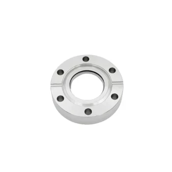
CF Ultra-High Vacuum Observation Window Window Flange High Borosilicate Glass Sight Glass
Discover CF ultra-high vacuum observation window flanges with high borosilicate glass, perfect for semiconductor manufacturing, vacuum coating, and optical instruments. Clear observation, durable design, easy installation.

CVD Diamond Optical Windows for Lab Applications
Diamond optical windows: exceptional broad band infrared transparency, excellent thermal conductivity & low scattering in infrared, for high-power IR laser & microwave windows applications.
No Demolding Lab Infrared Press Mold for Laboratory Applications
Effortlessly test your samples with no demolding required using our lab infrared press mold. Enjoy high transmittance and customizable sizes for your convenience.

Silicon Carbide (SIC) Ceramic Sheet Wear-Resistant Engineering Advanced Fine Ceramics
Silicon carbide (sic) ceramic sheet is composed of high-purity silicon carbide and ultra-fine powder, which is formed by vibration molding and high-temperature sintering.
Optical Window Glass Substrate Wafer Single Double Sided Coated K9 Quartz Sheet
K9 glass, also known as K9 crystal, is a type of optical borosilicate crown glass renowned for its exceptional optical properties.
Optical Window Glass Substrate Wafer CaF2 Substrate Window Lens
A CaF2 window is an optical window made of crystalline calcium fluoride. These windows are versatile, environmentally stable and resistant to laser damage, and they exhibit a high, stable transmission from 200 nm to about 7 μm.

Silicon Carbide (SIC) Ceramic Plate for Engineering Advanced Fine Ceramics
Silicon nitride (sic) ceramic is an inorganic material ceramic that does not shrink during sintering. It is a high-strength, low-density, high-temperature-resistant covalent bond compound.

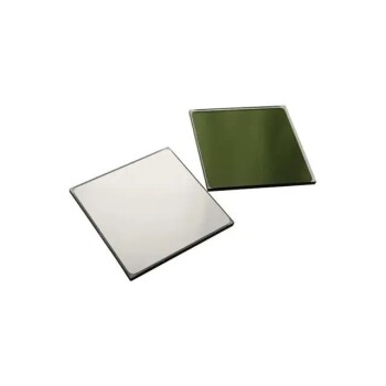
400-700nm Wavelength Anti Reflective AR Coating Glass
AR coatings are applied on optical surfaces to reduce reflection. They can be a single layer or multiple layers that are designed to minimize reflected light through destructive interference.

MgF2 Magnesium Fluoride Crystal Substrate Window for Optical Applications
Magnesium fluoride (MgF2) is a tetragonal crystal that exhibits anisotropy, making it imperative to treat it as a single crystal when engaging in precision imaging and signal transmission.

Infrared Transmission Coating Sapphire Sheet Substrate Window
Crafted from sapphire, the substrate boasts unparalleled chemical, optical, and physical properties. Its remarkable resistance to thermal shocks, high temperatures, sand erosion, and water sets it apart.
Optical Ultra-Clear Glass Sheet for Laboratory K9 B270 BK7
Optical glass, while sharing many characteristics with other types of glass, is manufactured using specific chemicals that enhance properties crucial for optics applications.

Precision Machined Silicon Nitride (SiN) Ceramic Sheet for Engineering Advanced Fine Ceramics
Silicon nitride plate is a commonly used ceramic material in the metallurgical industry due to its uniform performance at high temperatures.

Optical Window Glass Substrate Wafer Quartz Plate JGS1 JGS2 JGS3
The quartz plate is a transparent, durable, and versatile component widely used in various industries. Made from high-purity quartz crystal, it exhibits excellent thermal and chemical resistance.
CF Ultra-High Vacuum Observation Window Stainless Steel Flange Sapphire Glass Sight Glass
Discover CF ultra-high vacuum observation windows with sapphire glass and stainless steel flanges. Ideal for semiconductor manufacturing, vacuum coating, and more. Clear observation, precise control.
KF Ultra-High Vacuum Observation Window Stainless Steel Flange Sapphire Glass Sight Glass
Discover the KF Ultra-High Vacuum Observation Window, featuring sapphire glass and stainless steel flange for clear, reliable observation in ultra-high vacuum environments. Ideal for semiconductor, vacuum coating, and scientific research applications
Related Articles

Comparison of Planar and Rotating Silicon Targets in Thin Film Deposition
An in-depth comparison of the advantages and disadvantages of planar and rotating silicon targets, focusing on their characteristics and application scenarios in thin film deposition technology.
Understanding Optical Filters
An overview of optical filters, their types, and applications.
Difference between Single Crystal Quartz and Fused Silica
A detailed comparison of single crystal quartz and fused silica across various properties and preparation methods.
Optical Filter Structures and Construction Methods
An overview of various optical filter structures and their construction methods, focusing on different coating techniques and assembly processes.