Introduction to Plasma-Enhanced Chemical Vapor Deposition (PECVD)
PECVD is a type of chemical vapor deposition process that uses plasma to enhance the chemical reactions between the gas-phase precursors and the substrate. The plasma is created by applying radio-frequency (RF) power to a gas, which ionizes the gas and generates high-energy electrons that collide with other gas molecules, creating a highly reactive plasma. PECVD allows for the deposition of thin films with excellent uniformity and conformality, making it an ideal process for the fabrication of microelectronic and optoelectronic devices. However, it also has some disadvantages, such as high equipment cost and the need for specialized training to operate the equipment.
Table of Contents
Advantages and Disadvantages of PECVD
Advantages of PECVD
The PECVD process has several advantages that make it a popular and effective technique for the deposition of thin films in a variety of applications. One of the main advantages is its ability to deposit a wide range of materials onto different substrates. Additionally, PECVD operates at a relatively low temperature, typically between 100°C and 400°C, which makes it suitable for depositing thin films onto temperature-sensitive materials. Furthermore, the films deposited by the PECVD process have good dielectric properties, low mechanical stress, and excellent uniformity.
Good dielectric properties
The PECVD process provides thin films with good dielectric properties, which make it a popular choice for integrated circuit fabrication. The transistor needs a good dielectric layer to maintain its characteristics and performance.
Low mechanical stress and excellent uniformity
The PECVD process can prevent the films being deformed and become non-uniform because of the uneven mechanical stress on the films. The films' thickness over the step edge and flat surface can be maintained uniform, which is a great advantage of the PECVD when the fabrication process requires high step coverage because some of the fabrication processes may have a substrate with several steps on the surface.
High deposition rate and scalability
PECVD provides high deposition rates, which are substantially higher than other, more traditional vacuum-based techniques, such as PVD. This is the basis for a reliable low-cost fabrication technology. PECVD is also highly scalable, making it suitable for large-scale production.
Disadvantages of PECVD
Despite its advantages, the PECVD process also has some disadvantages. One of the main disadvantages is its high cost compared to other thin film deposition techniques. Additionally, the PECVD process is sensitive to the quality of the precursor gases used, which can affect the quality of the deposited films. Furthermore, the plasma gases used during the PECVD process can react with silicon or nitrogen to form Si-H and SiNH, affecting the properties of the devices, including UV absorption, stability, mechanical stress, and electrical conductivity. Finally, the plasma system ionizes the gases and drives them in a certain direction to deposit the material, which can sometimes damage the films or devices and deteriorate their performance during the process.
In conclusion, the PECVD process is a widely used technique in the field of materials science and engineering due to its ability to deposit a wide range of materials onto different substrates, its high deposition rate, and its scalability. It also provides thin films with good dielectric properties, low mechanical stress, and excellent uniformity. However, the PECVD process also has some disadvantages, including its high cost, sensitivity to the quality of the precursor gases used, and the potential for plasma damage to the films or devices.
Understanding Plasma in PECVD Process
Plasma is an essential component of the PECVD process as it plays a crucial role in the deposition of thin films on semiconductors. The plasma is generated by applying a high-frequency electric field to a gas, such as hydrogen or nitrogen. This causes the gas to ionize and form a plasma, which contains ions, electrons, and excited neutral atoms.
Importance of Plasma in PECVD Process
The plasma in the PECVD process is essential to achieving high-quality and uniform thin films. It activates the precursors and promotes the chemical reaction that forms the thin film. The reactive species in the plasma can then interact with the precursors that are introduced into the reaction chamber to form the thin film.
Plasma Generation in PECVD Process
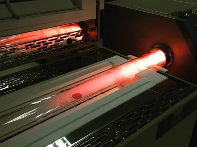
The PECVD process uses electrical energy to create a glow discharge, which is plasma. The plasma is achieved by having a Radio frequency (RF) in the alternating current range discharge between two electrodes. The space in between the two electrodes has gasses which use the RF energy to ionize and transform the various gasses that are in the PECVD chamber into reactive radicals, ions, neutral atoms, and molecules.
Composition of Plasma
Plasma is a partially ionized gas, which means that some electrons are free, leaving atoms with positive and negative charges. Plasma responds very well to electromagnetic fields, and it has characteristics of solids, liquids, and gases, making it a distinct state of matter. The reactive species in the plasma include ions, electrons, and excited neutral atoms that can then interact with the precursors and form the thin film.
Optimizing the Plasma in PECVD Process
The PECVD process can be optimized by controlling the gas flow rate, temperature, pressure, and power of the plasma. The plasma parameters, such as the form of the radicals, their flux onto the film-growing surface, and the surface reactions activated by substrate heating, affect the structure and properties of thin films.
Advantages of Plasma in PECVD Process
One of the main advantages of the PECVD process is that it can deposit high-quality and uniform thin films at a relatively low temperature. This makes it ideal for depositing materials that are temperature-sensitive or that get their characteristics changed at high temperatures. The PECVD process is widely used in the semiconductor, optoelectronics, and solar cell industries.
In conclusion, understanding the plasma in the PECVD process is crucial to achieving successful thin film deposition, and optimizing the process parameters is essential to achieving high-quality and uniform thin films.
Steps to Prepare for PECVD Process
The Plasma Enhanced Chemical Vapor Deposition (PECVD) process is a powerful technique used to deposit thin films of materials onto a substrate, and proper preparation is essential to ensure the quality and uniformity of the deposited film. In this section, we'll provide a step-by-step guide to the preparation process of PECVD.
Step 1: Clean the Substrate
The first step in preparing for the PECVD process is to clean the substrate thoroughly. Any contaminants on the substrate can negatively impact the quality of the deposited film, so it's essential to ensure that the substrate is completely clean. This can be achieved through various cleaning techniques, such as solvent cleaning, plasma cleaning, or wet chemical cleaning.
Step 2: Load the Substrate into the PECVD Chamber
Once the substrate is clean, the next step is to load it into the PECVD chamber. It's critical to ensure that the substrate is appropriately positioned in the chamber, as this can affect the quality and uniformity of the deposited film. The substrate should be placed on a holder that is compatible with the PECVD system and positioned at the optimum distance from the plasma source.
Step 3: Evacuate the Chamber to a Vacuum
After the substrate is loaded, the chamber is then evacuated to a vacuum. This is necessary to remove any residual gases that could interfere with the PECVD process. The vacuum level required will depend on the specific PECVD system being used, but typically it will be in the range of 1-10 mTorr.
Step 4: Introduce the Precursor Gases
Once the vacuum is achieved, the PECVD process can begin. This involves introducing the precursor gases into the chamber, which will then be ionized by the plasma source to form the thin film. The specific precursor gases and process parameters used will depend on the material being deposited and the desired film properties.
Step 5: Monitor the Process
During the PECVD process, it's essential to monitor the process parameters carefully to ensure that the deposition is proceeding as desired. Parameters such as temperature, pressure, and gas flow rates should be monitored and adjusted as necessary to achieve the desired film properties.
Step 6: End the Process
Once the deposition is complete, the PECVD process can be ended by stopping the flow of precursor gases and allowing the chamber to return to atmospheric pressure. The substrate can then be removed from the chamber and further processed as needed.
In conclusion, proper preparation is crucial to ensure the quality and uniformity of the thin films deposited using the PECVD process. By following the steps outlined above, you can ensure that you're fully prepared for the PECVD process and achieve the desired film properties.
Monitoring and Controlling the Deposition
During the PECVD process, it is important to monitor and control the deposition to ensure the quality and uniformity of the deposited film. The following are the steps involved in monitoring and controlling the deposition process:
Step 1: Determine the appropriate process parameters
The first step in the process is to determine the appropriate process parameters, including gas flow rates, pressure, and power settings. These parameters need to be set according to the desired film properties.
Step 2: Begin the deposition process
Once the appropriate process parameters have been set, the deposition process can begin. During the process, it is important to monitor the deposition rate and film thickness using various techniques such as ellipsometry or profilometry.
Step 3: Real-time monitoring
Real-time monitoring can help to identify any potential issues that may arise during the deposition process, such as non-uniformity or contamination. In-situ diagnostics such as optical emission spectroscopy or mass spectrometry can provide information about the plasma chemistry and help to optimize the deposition process.
Step 4: Adjust the process parameters as needed
To control the deposition, the gas flow rates, pressure, and power settings can be adjusted as needed. This can be done based on the real-time monitoring results.
Step 5: Post-deposition analysis
Post-deposition analysis can be done to verify the film properties and quality. This can be done using techniques such as X-ray diffraction, scanning electron microscopy, and atomic force microscopy.
In conclusion, monitoring and controlling the deposition during the PECVD process is critical for achieving high-quality thin films with uniform thickness and properties. The process involves determining the appropriate process parameters, real-time monitoring, adjusting the process parameters as needed, and post-deposition analysis.
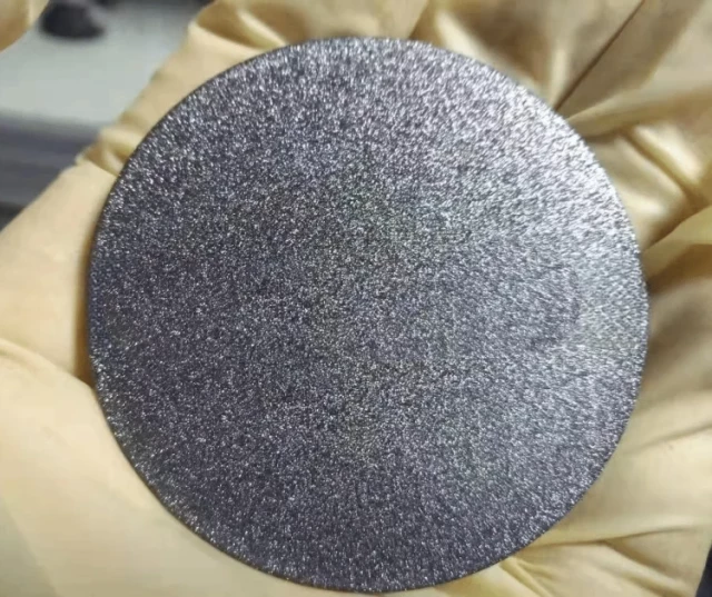
PECVD Film Post-Treatment
Once the PECVD thin film is deposited, it requires post-treatment to improve its properties and performance. The post-treatment process can involve annealing, etching, or other methods depending on the specific application.
Annealing
Annealing is a commonly used post-treatment method for PECVD films. It involves heating the film to a high temperature in a controlled environment to improve its crystallinity, density, and adhesion to the substrate. Annealing can also help to remove any residual stress in the film and improve its mechanical properties.
Etching
Etching is used to remove unwanted material from the film surface, such as impurities or defects. The choice of etching method depends on the specific application of the PECVD film. Wet etching is a common method used for removing unwanted material from the surface of the film. Dry etching, on the other hand, is used for more precise and controlled removal of material from the film surface.
Other Methods
Other post-treatment methods for PECVD films include ion implantation, chemical mechanical polishing, and surface modification. Ion implantation is used to alter the electrical and mechanical properties of the film by introducing impurities into the film. Chemical mechanical polishing is used to remove any unwanted material from the surface of the film using a combination of chemical and mechanical processes. Surface modification involves altering the surface of the film to improve its properties, such as its adhesion, wettability, or biocompatibility.
In conclusion, the post-treatment of PECVD films is essential to improve their properties and performance. The choice of post-treatment method depends on the specific application of the film. Annealing and etching are the most commonly used post-treatment methods for PECVD films. However, other methods, such as ion implantation, chemical mechanical polishing, and surface modification, may also be used depending on the requirements of the film.
Conclusion and Future of PECVD
PECVD is an essential process for depositing thin films in various applications, including microelectronics, optics, and sensors. Despite its advantages, such as low-temperature deposition and high uniformity, PECVD has some disadvantages, such as low deposition rate and high equipment cost. However, ongoing research aims to improve the process by developing new precursors and optimizing the deposition conditions. In the future, PECVD is expected to play a crucial role in the development of advanced technologies, such as the Internet of Things (IoT), wearable devices, and flexible electronics.
Related Products
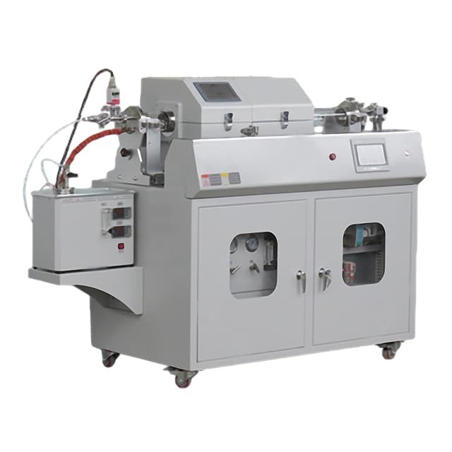
- Inclined Rotary Plasma Enhanced Chemical Vapor Deposition PECVD Equipment Tube Furnace Machine
- Chemical Vapor Deposition CVD Equipment System Chamber Slide PECVD Tube Furnace with Liquid Gasifier PECVD Machine
- Inclined Rotary Plasma Enhanced Chemical Vapor Deposition PECVD Equipment Tube Furnace Machine
- RF PECVD System Radio Frequency Plasma-Enhanced Chemical Vapor Deposition RF PECVD
- Multi Heating Zones CVD Tube Furnace Machine Chemical Vapor Deposition Chamber System Equipment
Related Articles
- Understanding Glow Discharge in the PECVD Process
- PECVD Furnace A Low-Power and Low-Temperature Solution for Soft Matter
- Types of PECVD Process, Equipment Structure, and Its Process Principle
- Comparing the Performance of PECVD and HPCVD in Coating Applications
- PECVD Technology: Principles, Materials, Advantages, and Applications


