Table of Contents
Introduction to PECVD
Plasma Enhanced Chemical Vapor Deposition (PECVD) is a thin film deposition technique widely used in the semiconductor industry. It combines the principles of chemical vapor deposition (CVD) with plasma technology to create high-quality thin films with precise control over their properties. Unlike conventional CVD, PECVD utilizes a plasma to enhance the deposition process, enabling the deposition of a wider range of materials at lower temperatures. This article provides a comprehensive guide to PECVD, exploring its principles, applications, advantages, and limitations. We will discuss the process flow, plasma sources, and key parameters involved in PECVD, as well as its role in semiconductor manufacturing and emerging applications in other industries.
Principle of PECVD
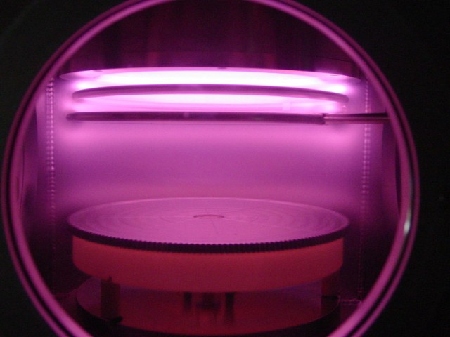
PECVD technology utilizes low-temperature plasma to induce a glow discharge at the cathode of the process chamber (i.e. the sample tray) under low air pressure. This glow discharge, or an alternative heat generator, elevates the sample's temperature to a predetermined level, after which a controlled amount of process gas is introduced. This gas undergoes a series of chemical and plasma reactions, culminating in the formation of a solid film on the sample's surface.
Plasma processes in thin film formation are typically employed in three primary modes: plasma etching, plasma grafting of new functional groups, and plasma-enhanced CVD.
Plasma-enhanced chemical vapor deposition (PECVD) stands out as a versatile fabrication technique that leverages plasma to enhance the reactivity of organic and inorganic chemical monomers for the deposition of thin films. This increased reactivity enables the utilization of a wide range of materials as precursors, encompassing those conventionally considered inert. PECVD offers the capability to employ precursors in solid, liquid, or gas form, facilitating the facile, rapid, and solvent-free fabrication of thin coatings.
High Density Plasma Enhanced Chemical Vapor Deposition (HDPECVD) takes place in deposition equipment that utilizes two power sources. One is a capacitively coupled plasma for bias power in direct contact with the substrate, while the other is the inductively coupled plasma as the source power for the external generator. The source power drives a more efficient breakdown of precursors, resulting in higher plasma density and reaction rates.
Other types of PECVD plasma sources include:
- Mid-frequency AC and pulsed DC: Used in large area industrial PECVD coating systems to drive a plasma either on two parallel electrodes or directly on the substrate itself. A common application is the deposition of SiOx onto parts for corrosion and hydrophobic coatings, using two electrodes and a high voltage mid-frequency AC discharge to drive the PECVD process.
- Pulsed DC bias: Typically applied to the parts themselves for DLC coatings. This creates a plasma around the parts, causing DLC to be deposited from acetylene or other hydrocarbon gases.
PECVD Applications and Materials
Plasma-enhanced chemical vapor deposition (PECVD) is a versatile deposition technique that offers precise control over the deposition process, enabling the production of thin films with tailored properties. This technology finds wide application in various industries, including but not limited to:
-
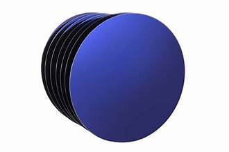
Semiconductor manufacturing: PECVD is extensively used in the fabrication of semiconductor devices, serving as a key deposition method for gate dielectrics, passivation layers, and interconnects.
-
Solar cell production: PECVD plays a pivotal role in the manufacturing of solar cells and photovoltaic devices. Its ability to deposit thin, uniform films over large surface areas makes it an ideal choice for creating anti-reflective coatings and other functional layers in solar panels.
-
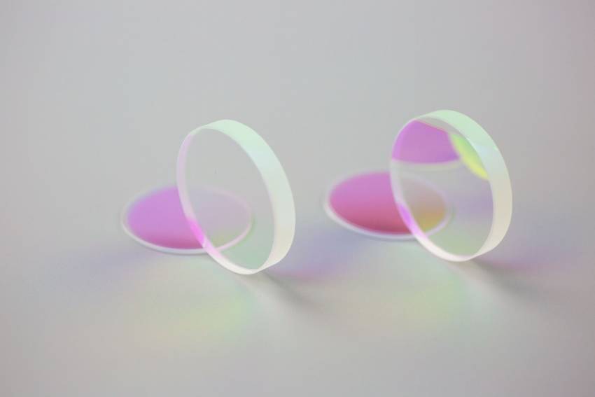
Optical coatings: PECVD is employed in the production of optical coatings, including those found in sunglasses, tinted optical devices, and photometers. By precisely controlling the plasma parameters, the refractive index and other optical properties of the deposited films can be finely tuned, resulting in coatings with desired optical characteristics.
-
Food packaging: PECVD is widely used in the food packaging industry, enabling the deposition of dense, inert coatings on packaging materials such as potato chip bags. These coatings provide excellent barrier properties, protecting the contents from moisture and oxygen infiltration, thereby extending product shelf life.
-
Biomedical devices: PECVD is utilized in the fabrication of biomedical devices, such as medical implants. The ability to deposit biocompatible, high-purity coatings with tailored properties makes PECVD an attractive choice for applications requiring biocompatibility and functionality.
Common PECVD Materials
A wide range of materials can be deposited using PECVD, including:
-
Silicon nitride (SiN): SiN is a common material deposited by PECVD, known for its excellent dielectric properties, high thermal stability, and low electrical conductivity. It finds application in semiconductor devices, biomedical devices, and optical coatings.
-
Silicon dioxide (SiO2): SiO2 is another frequently deposited material in PECVD. It is a transparent dielectric material with good electrical insulation properties. SiO2 is widely used in semiconductor manufacturing, optical coatings, and protective layers.
-
Amorphous silicon (a-Si): a-Si is a non-crystalline form of silicon with unique electronic properties. It is used in the production of thin-film solar cells, photodetectors, and display devices.
-
Diamond-like carbon (DLC): DLC is a carbon-based material with properties similar to diamond, including high hardness and low friction. PECVD is employed to deposit DLC coatings for applications such as cutting tools, wear-resistant surfaces, and biomedical implants.
-
Metals: PECVD can also be used to deposit metallic films, such as aluminum and copper. These films find application in electrical interconnects, electrodes, and other electronic components.
PECVD Process Parameters
Plasma-enhanced chemical vapor deposition (PECVD) is a thin-film deposition technique that uses a plasma to enhance the chemical reactions involved in the deposition process. PECVD is widely used in the semiconductor industry to deposit a variety of materials, including silicon nitride, silicon dioxide, and polysilicon.
The key process parameters in PECVD include:
- Pressure: The pressure in the deposition chamber affects the mean free path of the reactive species and the rate of deposition.
- Temperature: The temperature of the substrate affects the surface mobility of the reactive species and the crystallinity of the deposited film.
- Gas flow rates: The flow rates of the precursor gases affect the composition and properties of the deposited film.
- Plasma power: The plasma power affects the energy of the plasma and the rate of deposition.
The optimization of PECVD process parameters is critical for achieving the desired film properties. For example, the deposition rate can be increased by increasing the plasma power or the flow rate of the precursor gases. The film thickness can be controlled by adjusting the deposition time. The film composition can be controlled by adjusting the flow rates of the precursor gases.
PECVD is a versatile thin-film deposition technique that can be used to deposit a wide range of materials with a variety of properties. By optimizing the process parameters, PECVD can be used to produce high-quality films for a variety of applications.
Challenges and Troubleshooting in PECVD
PECVD is a complex process, and there are a number of challenges that can arise during deposition. These challenges include:
- Non-uniformity: The deposited film may not be uniform in thickness or composition across the substrate.
- Pinholing: The deposited film may contain pinholes, which are small holes that can allow gases or liquids to pass through the film.
- Cracking: The deposited film may crack if it is subjected to excessive stress.
- Contamination: The deposited film may be contaminated with impurities from the process gases or the deposition chamber.
These challenges can be overcome by optimizing the process parameters and by using proper troubleshooting techniques. For example, non-uniformity can be reduced by increasing the substrate temperature or by using a rotating substrate holder. Pinholing can be reduced by increasing the deposition pressure or by using a higher-purity precursor gas. Cracking can be reduced by decreasing the deposition rate or by using a substrate with a lower coefficient of thermal expansion. Contamination can be reduced by using a cleaner deposition chamber and by using higher-purity precursor gases.
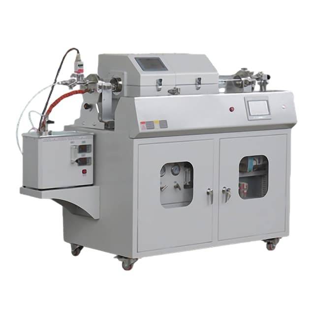
PECVD Equipment and Systems
PECVD (Plasma Enhanced Chemical Vapor Deposition) equipment and systems are essential tools in modern semiconductor manufacturing. They offer excellent film uniformity, low-temperature processing, and high throughput. These systems are used in various applications, including the deposition of thin films for microelectronic devices, photovoltaic cells, and display panels.
Types of PECVD Reactors
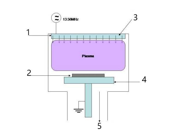
PECVD reactors can be classified based on the method used to generate plasma:
-
Capacitively Coupled Plasma (CCP): Plasma is generated between two electrodes, with the substrate placed on one of the electrodes.
-
Inductively Coupled Plasma (ICP): Plasma is generated using an induction coil wrapped around the deposition chamber.
-
Microwave Plasma (MWP): Plasma is generated using microwaves.
Plasma Generation Methods
Plasma in PECVD processes is typically generated by applying a voltage to electrodes embedded in a gas at low pressures. PECVD systems can generate plasma by different means, including radio frequency (RF), mid-frequencies (MF), pulsed DC, or straight DC power. The energy supplied by the power source activates the gas or vapor, forming electrons, ions, and neutral radicals.
In-situ Monitoring and Control Systems
In-situ monitoring and control systems are essential for ensuring the quality and uniformity of PECVD films. These systems can monitor various parameters, including:
- Plasma parameters (e.g., electron density, ion energy)
- Gas flow rates
- Temperature
- Film thickness
By monitoring and controlling these parameters, PECVD systems can optimize the deposition process and produce high-quality films with precise control over their properties.
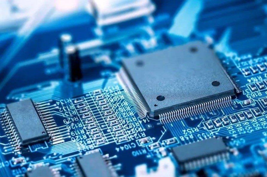
PECVD Applications in Semiconductor Manufacturing
Plasma-enhanced chemical vapor deposition (PECVD) is a critical process in modern semiconductor manufacturing, enabling the deposition of functional thin films with controlled thickness, chemical composition, and properties. PECVD offers several advantages over conventional chemical vapor deposition (CVD) techniques, including excellent film uniformity, low-temperature processing, and high throughput.
Role of PECVD in Semiconductor Fabrication
PECVD plays a crucial role in the fabrication of various semiconductor components. Its applications include:
-
Gate Oxide Deposition: PECVD is used to deposit high-quality gate oxides in metal-oxide-semiconductor (MOS) transistors. These oxides act as insulators between the gate electrode and the semiconductor channel, controlling the flow of current in the device.
-
Passivation Layers: PECVD is employed to deposit passivation layers over semiconductor devices to protect them from environmental contaminants and improve device reliability. These layers typically consist of silicon nitride or silicon dioxide and prevent the diffusion of impurities and moisture into the semiconductor.
-
Interconnect Formation: PECVD is used to deposit metal interconnects in integrated circuits (ICs). These interconnects provide electrical connections between different components on the chip and are typically made of materials such as copper or aluminum.
Advantages of PECVD for Semiconductor Applications
PECVD offers several advantages for semiconductor applications:
-
Low-Temperature Processing: PECVD can deposit thin films at temperatures significantly lower than conventional CVD techniques. This is crucial for semiconductor manufacturing, as high temperatures can damage delicate device structures.
-
Excellent Film Uniformity: PECVD produces highly uniform thin films with consistent thickness and composition across the substrate surface. This uniformity is essential for ensuring device performance and reliability.
-
High Deposition Rates: PECVD offers high deposition rates compared to conventional CVD techniques, enabling efficient and cost-effective manufacturing of semiconductor devices.
-
Wide Range of Materials: PECVD can deposit a wide range of materials, including insulators, conductors, and semiconductors. This versatility makes it suitable for various applications in semiconductor manufacturing.
-
In-situ Process Control: PECVD systems often incorporate in-situ process monitoring and control capabilities, allowing for real-time adjustment of deposition parameters to optimize film properties.
Conclusion
PECVD is a critical process in modern semiconductor manufacturing, offering a unique combination of advantages such as low-temperature processing, excellent film uniformity, high deposition rates, and a wide range of materials. As the demand for advanced electronic devices continues to grow, PECVD systems will play an increasingly significant role in the semiconductor industry.
Future Trends in PECVD
Plasma Enhanced Chemical Vapor Deposition (PECVD) is a thin-film deposition technique that combines plasma energy with chemical vapor deposition (CVD). This hybrid process offers several advantages over traditional CVD, including lower deposition temperatures, higher deposition rates, and improved film properties.
As a result, PECVD is increasingly being used in the manufacture of a wide range of electronic devices, including semiconductors, photovoltaic cells, and display panels.

In the future, PECVD is expected to continue to play an important role in the electronics industry. Several emerging applications and advancements are driving the growth of the PECVD market, including:
- New materials: PECVD can be used to deposit a wide range of materials, including metals, semiconductors, dielectrics, and polymers. This versatility makes PECVD an attractive option for a variety of applications, including advanced packaging, photonics, and microelectronics.
- Integration with other deposition techniques: PECVD can be integrated with other deposition techniques, such as physical vapor deposition (PVD) and atomic layer deposition (ALD), to create complex multilayer structures. This integration enables the fabrication of devices with tailored properties and improved performance.
- Research and development: Ongoing research and development is focused on improving the performance of PECVD systems and expanding their range of applications. This research is expected to lead to the development of new PECVD processes and materials that will enable the fabrication of next-generation devices.
The PECVD market is expected to grow significantly in the coming years. This growth will be driven by the increasing demand for advanced electronic devices, the development of new materials and processes, and the integration of PECVD with other deposition techniques.
Related Products
- RF PECVD System Radio Frequency Plasma-Enhanced Chemical Vapor Deposition RF PECVD
- Inclined Rotary Plasma Enhanced Chemical Vapor Deposition PECVD Equipment Tube Furnace Machine
- Inclined Rotary Plasma Enhanced Chemical Vapor Deposition PECVD Equipment Tube Furnace Machine
- Chemical Vapor Deposition CVD Equipment System Chamber Slide PECVD Tube Furnace with Liquid Gasifier PECVD Machine
- Microwave Plasma Chemical Vapor Deposition MPCVD Machine System Reactor for Lab and Diamond Growth


