At its core, sputtering is a superior deposition method due to its exceptional material versatility, the high quality of the films it produces, and the precise control it offers over the entire process. Unlike thermal methods that rely on melting and evaporation, sputtering is a physical process that uses energized ions to physically dislodge atoms from a target material, which then deposit onto a substrate, creating dense, highly adherent, and pure thin films.
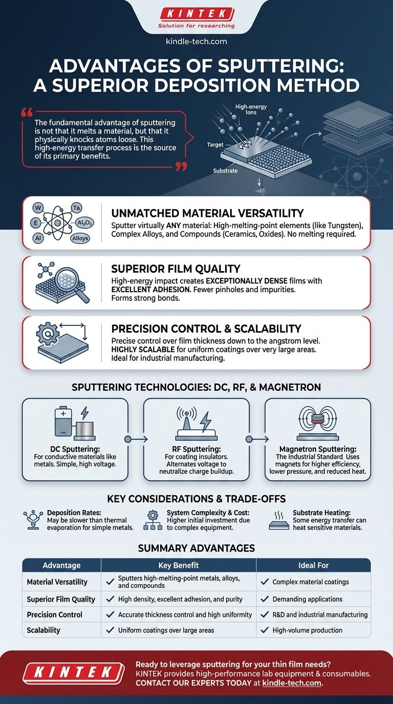
The fundamental advantage of sputtering is not that it melts a material, but that it physically knocks atoms loose. This high-energy transfer process is the source of its primary benefits: the ability to coat with virtually any material and the creation of films with unparalleled density and adhesion.
Why Sputtering Excels: The Core Principles
Sputtering's advantages stem directly from its underlying physical vapor deposition (PVD) mechanism. Understanding this mechanism is key to appreciating its capabilities.
Unmatched Material Versatility
Because sputtering does not require melting the source material, it can be used for an incredibly broad range of substances.
This includes high-melting-point elements (like tungsten or tantalum), complex alloys, and compounds (like ceramics or oxides) that would decompose or separate if heated to their evaporation point.
Superior Film Quality
The atoms dislodged from the sputtering target travel with significant kinetic energy. When they strike the substrate, they don't just gently land; they embed themselves, creating an exceptionally strong bond.
This high-energy impact results in films that are extremely dense, with fewer pinholes or impurities compared to other methods. The resulting adhesion to the substrate is excellent, often forming a thin diffusion layer that locks the film in place.
Precision Control and Scalability
Sputtering is a highly controllable and repeatable process. Key parameters like the sputtering rate are directly managed by adjusting the electrical current to the target.
This allows for precise control over film thickness down to the angstrom level. The process is also highly scalable, capable of producing uniform coatings over very large areas, making it a cornerstone of industrial manufacturing for everything from semiconductors to architectural glass.
Understanding Sputtering Technologies: DC, RF, and Magnetron
While the principle is the same, different sputtering techniques are used to handle different materials and improve efficiency.
DC Sputtering: The Foundation
Direct Current (DC) sputtering is the simplest form. A high DC voltage is applied to a conductive target material. This is effective and straightforward but is limited to electrically conductive materials like metals.
RF Sputtering: Coating Insulators
When sputtering insulators or semiconductors, a positive charge builds up on the target surface, repelling the positive ions and stopping the process.
Radio Frequency (RF) sputtering alternates the voltage at high frequency. This alternating field attracts electrons to neutralize the charge buildup, allowing for the effective sputtering of non-conductive dielectric materials.
Magnetron Sputtering: The Industrial Standard
Magnetron sputtering is the most widely used technique today. It adds powerful magnets behind the target material.
These magnets trap electrons in a magnetic field directly in front of the target, dramatically increasing the efficiency of ion formation in the plasma. This results in a much higher deposition rate, allows the process to run at lower pressures and temperatures, and reduces potential damage to heat-sensitive substrates.
Key Considerations and Trade-offs
No technology is perfect for every scenario. To make an informed decision, you must understand the limitations of sputtering.
Deposition Rates
While magnetron sputtering offers high rates for many materials, traditional thermal evaporation can sometimes be faster for depositing simple, low-melting-point metals like aluminum. The choice often depends on whether speed or film quality is the primary driver.
System Complexity and Cost
Sputtering systems are more complex than simple evaporators. They require a robust vacuum chamber, high-voltage power supplies (DC or RF), process gas control, and, for magnetron systems, powerful magnets. This translates to a higher initial equipment cost.
Substrate Heating
Although magnetron sputtering is considered a "low temperature" process, the high-energy bombardment of atoms does transfer some heat to the substrate. For extremely sensitive organic materials or devices, this energy transfer must be carefully managed.
Making the Right Choice for Your Application
Selecting the right deposition technique depends entirely on your end goal and the materials you are working with.
- If your primary focus is film quality, adhesion, and density: Sputtering is the definitive choice, as the high-energy deposition process is inherently superior.
- If your primary focus is depositing high-melting-point metals, complex alloys, or compounds: Sputtering is one of the only viable and controllable methods available.
- If your primary focus is coating a non-conductive ceramic or oxide: You must use RF sputtering to overcome the effects of charge buildup on the target.
- If your primary focus is industrial-scale production with high uniformity over large areas: Magnetron sputtering provides the speed, control, and scalability required for manufacturing.
By understanding these core principles and trade-offs, you can confidently leverage sputtering to achieve superior material performance and reliability in your application.
Summary Table:
| Advantage | Key Benefit | Ideal For |
|---|---|---|
| Material Versatility | Sputters high-melting-point metals, alloys, and compounds | Complex material coatings |
| Superior Film Quality | High density, excellent adhesion, and purity | Demanding applications requiring reliability |
| Precision Control | Accurate thickness control and high uniformity | R&D and industrial manufacturing |
| Scalability | Uniform coatings over large areas | High-volume production |
Ready to leverage sputtering for your thin film needs? KINTEK specializes in high-performance lab equipment and consumables for all your deposition challenges. Whether you're working with advanced alloys, ceramics, or require industrial-scale uniformity, our solutions deliver the precision and reliability you need. Contact our experts today to discuss how we can enhance your coating process!
Visual Guide
Related Products
- Lab Sterile Slapping Type Homogenizer for Tissue Mashing and Dispersing
- Spark Plasma Sintering Furnace SPS Furnace
- Single Punch Manual Tablet Press Machine TDP Tablet Punching Machine
People Also Ask
- Why is it necessary to use an ultrasonic cell disruptor before yeast flow cytometry? Ensure Data Accuracy
- Why is maintaining nanoparticle dispersion critical for photocatalytic reactors? Maximize Your Reaction Efficiency
- What role does a laboratory homogenizer play in radioactive cesium detection? Ensure Accuracy in Wildlife Sampling
- How does a laboratory automatic masticator or homogenizer facilitate the processing of biofilm samples? Optimize Accuracy
- What is the primary function of an ultrasonic cleaner in coating? Achieve Unmatched Substrate Purity for PVD Adhesion


