In short, sputtering is a foundational technology used to apply ultra-thin functional coatings onto other materials. Its applications range from creating the microscopic layers in computer chips and coating medical implants to producing anti-reflection layers on eyeglasses and specialized films for solar cells.
The true value of sputtering is not in any single application, but in its remarkable versatility. It provides a precise, controllable method for depositing a vast range of materials as exceptionally smooth and durable thin films, enabling advancements across nearly every high-tech industry.
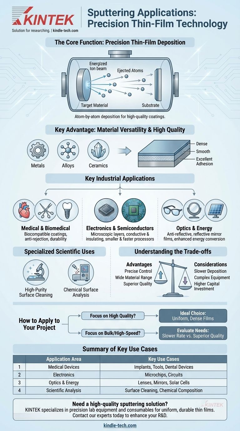
The Core Function: Precision Thin-Film Deposition
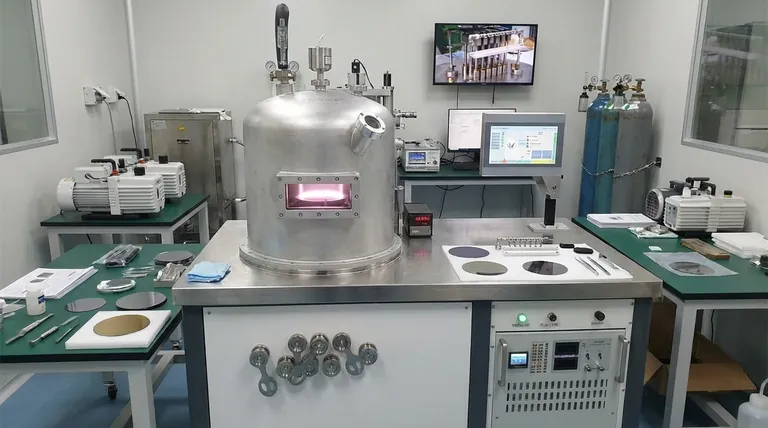
Sputtering is a type of Physical Vapor Deposition (PVD), a process that takes place inside a high-vacuum chamber. Its primary purpose is to create high-quality coatings at an atomic level.
How Sputtering Creates a Coating
The process involves bombarding a source material, called a target, with energized ions from a gas like argon. This bombardment has enough energy to knock atoms loose from the target material. These ejected atoms then travel through the vacuum and deposit onto a substrate, gradually building a thin, uniform film.
The Key Advantage: Material Versatility
One of sputtering's most significant advantages is its ability to work with an enormous variety of materials. It can deposit pure metals, alloys, and even insulating materials like ceramics that are difficult or impossible to deposit using other methods. By introducing reactive gases like oxygen or nitrogen, it can also form highly durable oxides and nitrides.
The Result: High-Quality Films
The films created through sputtering are known for their superior qualities. They are typically very dense, smooth, and have excellent adhesion to the substrate. This control over the film's structure makes it ideal for applications where performance and reliability are critical.
Key Industrial Applications
The unique capabilities of sputtering have made it indispensable in fields that rely on advanced materials and microfabrication.
Medical and Biomedical Devices
Sputtering is crucial for applying biocompatible or functional coatings to medical devices. These coatings improve performance and patient safety. Examples include anti-rejection coatings on implants, durable layers on surgical tools, and coatings for dental implants and angioplasty devices.
Electronics and Semiconductors
The modern electronics industry would not exist without sputtering. It is used to deposit the conductive and insulating layers that form the microscopic circuits on silicon wafers. This enables the creation of smaller, faster, and more powerful processors and memory chips.
Optics and Energy
In optics, sputtering is used to apply anti-reflective coatings to lenses and glasses, improving clarity and light transmission. It is also used to create highly reflective mirror coatings and specialized films for solar cells, where "better absorbers" are needed to enhance energy conversion efficiency.
Beyond Coatings: Specialized Scientific Uses
While thin-film deposition is its primary use, the underlying physical process of sputtering is also leveraged for other high-precision tasks.
High-Purity Surface Cleaning
The same ion bombardment used to eject atoms from a target can be directed at a substrate. This allows researchers to meticulously clean a surface, removing contaminants atom by atom to prepare a perfectly pure foundation for subsequent processes.
Chemical Surface Analysis
By capturing and analyzing the particles ejected from a target, scientists can determine the precise chemical composition of a material's surface. This technique provides valuable insights for materials research and quality control.
Understanding the Trade-offs
Despite its advantages, sputtering is not a universal solution. It is a high-vacuum process, which inherently brings two key considerations.
Deposition Speed
Sputtering is generally a slower deposition process compared to some other methods, like thermal evaporation. This makes it less suitable for applications requiring very thick films or extremely high throughput for low-cost items.
Equipment Complexity
The need for a high-vacuum environment, high-voltage power supplies, and process gas controls means that sputtering systems are complex and represent a significant capital investment. The process requires skilled operators to manage and maintain the equipment for optimal results.
How to Apply This to Your Project
Deciding if sputtering is the right approach depends entirely on your end goal and material requirements.
- If your primary focus is creating highly uniform, dense, and smooth films for sensitive applications: Sputtering is an ideal choice, offering unparalleled control over film properties for optics, electronics, or medical devices.
- If your primary focus is depositing complex alloys or insulating compounds: The versatility of sputtering allows you to work with materials that are impossible to handle with many alternative coating methods.
- If your primary focus is high-speed, bulk coating on simple parts: You should evaluate whether sputtering's superior film quality justifies its slower deposition rate and higher cost compared to other industrial coating techniques.
Ultimately, sputtering’s value lies in its precise control over material deposition, enabling the creation of advanced materials and devices from the atom up.
Summary Table:
| Application Area | Key Use Cases |
|---|---|
| Medical Devices | Biocompatible coatings for implants, surgical tools, dental devices |
| Electronics & Semiconductors | Conductive and insulating layers for microchips and circuits |
| Optics & Energy | Anti-reflective coatings for lenses, mirror films, solar cell layers |
| Scientific Analysis | High-purity surface cleaning, chemical composition analysis |
Need a high-quality sputtering solution for your lab? KINTEK specializes in precision lab equipment and consumables, including advanced sputtering systems. Our expertise ensures you achieve the uniform, durable thin films required for cutting-edge research and development in electronics, medical devices, and renewable energy. Contact our experts today to discuss how we can support your specific coating challenges and enhance your laboratory's capabilities.
Visual Guide
Related Products
- Spark Plasma Sintering Furnace SPS Furnace
- Vacuum Induction Melting Spinning System Arc Melting Furnace
- Chemical Vapor Deposition CVD Equipment System Chamber Slide PECVD Tube Furnace with Liquid Gasifier PECVD Machine
- Customer Made Versatile CVD Tube Furnace Chemical Vapor Deposition Chamber System Equipment
People Also Ask
- What is the difference between spark plasma sintering and flash sintering? A Guide to Advanced Sintering Methods
- What technical advantages does a Spark Plasma Sintering (SPS) furnace offer for LZP ceramics? Enhance Ionic Conductivity
- What is the process fundamentals of spark plasma sintering? Achieve Rapid, High-Density Material Consolidation
- What is the theory of spark plasma sintering? A Guide to Rapid, Low-Temperature Densification
- What are the advantages of CAMI/SPS for W-Cu composite preparation? Reduce cycles from hours to seconds.


