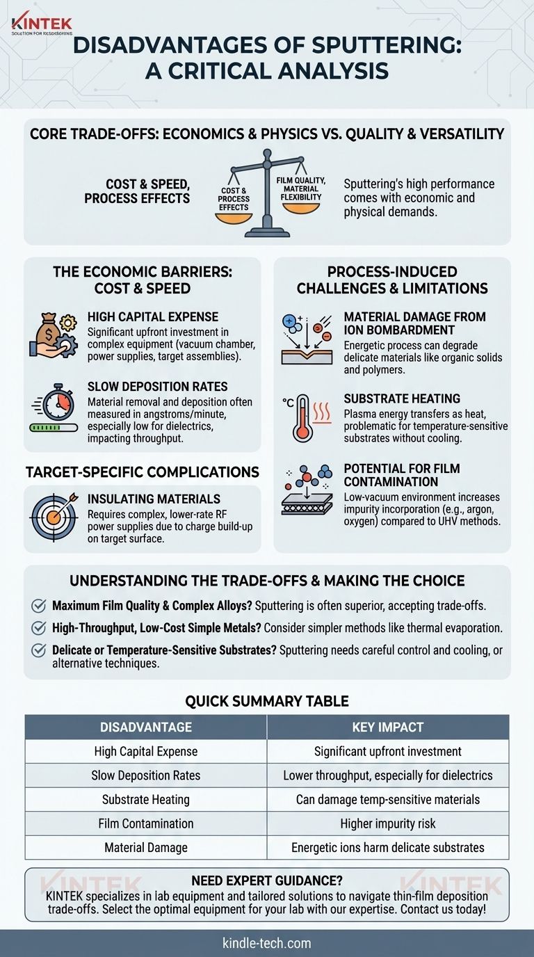
At its core, the primary disadvantages of sputtering are its high equipment cost, relatively slow deposition speed for certain materials, potential to damage sensitive substrates, and a higher risk of film contamination compared to ultra-high vacuum techniques. These factors represent a fundamental trade-off between sputtering's versatility and the economic and physical demands of the process.
Sputtering is an exceptionally powerful and versatile thin-film deposition technique, but it is not a universal solution. Its disadvantages primarily revolve around economic factors (cost and speed) and process-induced effects (heat, material damage, and impurities) that must be carefully weighed against its superior film quality and material flexibility.

The Economic Barriers: Cost and Speed
The decision to use sputtering often begins with an economic calculation. The initial investment and ongoing operational speed are significant considerations that can make or break its feasibility for a given project.
High Capital Expense
Sputtering systems are complex and require a significant upfront investment. The core components—including the vacuum chamber, high-power DC or RF power supplies, gas flow controllers, and target material assemblies—are all expensive. This initial cost can be a major barrier compared to simpler methods like thermal evaporation.
Slow Deposition Rates
While effective, sputtering can be a slow process. The rate at which material is removed from the target and deposited on the substrate is often measured in angstroms or nanometers per minute. For materials like dielectric insulators (e.g., SiO₂), which require RF sputtering, the rates can be even lower than for metals, impacting throughput in a production environment.
Process-Induced Challenges and Limitations
Beyond the economics, the physics of the sputtering process itself introduce several challenges that must be managed to achieve the desired film properties.
Material Damage from Ion Bombardment
Sputtering is an energetic, physical process. High-energy ions bombard the target to eject atoms, and the substrate is also exposed to this energetic environment. This can be detrimental to delicate materials, such as organic solids or certain polymers, which can degrade or be structurally damaged upon exposure to the plasma.
Substrate Heating
A significant amount of energy from the plasma is transferred to the substrate as heat. This temperature rise can be problematic for temperature-sensitive substrates, such as plastics, or when depositing films for biological applications. Without active substrate cooling, this heating can alter the substrate's properties or the characteristics of the film itself.
Potential for Film Contamination
Sputtering typically operates in a low-vacuum environment (higher pressure) compared to techniques like molecular beam epitaxy or even thermal evaporation. This means more residual gas atoms from the chamber atmosphere (e.g., argon, oxygen, nitrogen) are present. These atoms can become incorporated into the growing film as impurities, which can alter its electrical, optical, or mechanical properties.
Target-Specific Complications
The type of material being sputtered introduces its own set of challenges. When sputtering insulating materials with a standard DC power supply, a positive charge builds up on the target surface, effectively stopping the process. This requires the use of more complex and expensive RF (Radio Frequency) power supplies, which can have lower deposition rates and introduce more heating.
Understanding the Trade-offs: Why Sputtering is Still Chosen
Despite these disadvantages, sputtering is a dominant technique in industry and research. Understanding its benefits clarifies why these trade-offs are often accepted.
Unmatched Adhesion and Film Density
The high kinetic energy of the sputtered atoms results in films that are typically much denser and have far superior adhesion to the substrate compared to evaporated films. This is critical for applications requiring durable and robust coatings.
Unparalleled Material Versatility
Sputtering can deposit virtually any material, including high-melting-point metals, refractory compounds, and complex alloys. Crucially, the composition of a sputtered alloy film is generally the same as the target, a feat that is extremely difficult to achieve with evaporation.
Superior Control and Uniformity
The process provides excellent, repeatable control over film thickness simply by controlling time and power. Furthermore, sputtering systems are capable of depositing highly uniform films over very large areas, which is essential for manufacturing semiconductors, optical filters, and architectural glass.
Making the Right Choice for Your Application
Choosing your deposition method requires balancing your technical requirements against process limitations and cost.
- If your primary focus is maximum film quality (adhesion, density) or depositing complex alloys and compounds: Sputtering is often the superior choice, and its disadvantages are a necessary trade-off for performance.
- If your primary focus is high-throughput, low-cost deposition of simple metals: A less complex method like thermal evaporation may be a more economical and faster solution.
- If your primary focus is depositing on delicate or temperature-sensitive substrates: Sputtering can work, but requires careful process control and cooling; otherwise, a non-plasma technique should be considered.
Ultimately, understanding these drawbacks empowers you to select sputtering for the right reasons and to engineer the process to mitigate its inherent challenges.
Summary Table:
| Disadvantage | Key Impact |
|---|---|
| High Capital Expense | Significant upfront investment in equipment |
| Slow Deposition Rates | Lower throughput, especially for dielectrics |
| Substrate Heating | Can damage temperature-sensitive materials |
| Film Contamination | Higher impurity risk compared to UHV methods |
| Material Damage | Energetic ions may harm delicate substrates |
Need expert guidance on choosing the right thin-film deposition method for your lab? KINTEK specializes in lab equipment and consumables, offering tailored solutions to help you navigate the trade-offs of sputtering and other techniques. Our team can help you select the optimal equipment to maximize film quality, control costs, and protect sensitive substrates. Contact us today to discuss your specific laboratory needs and discover how KINTEK can enhance your research and production processes!
Visual Guide
Related Products
- Lab Sterile Slapping Type Homogenizer for Tissue Mashing and Dispersing
- Spark Plasma Sintering Furnace SPS Furnace
- Single Punch Manual Tablet Press Machine TDP Tablet Punching Machine
People Also Ask
- Why is it necessary to use an ultrasonic cell disruptor before yeast flow cytometry? Ensure Data Accuracy
- What role does a laboratory homogenizer play in radioactive cesium detection? Ensure Accuracy in Wildlife Sampling
- What is the primary function of an ultrasonic cleaner in coating? Achieve Unmatched Substrate Purity for PVD Adhesion
- What role does an ultrasonic cleaner play in the pre-treatment of 4140 steel? Ensure Uniform Nitriding Activation
- Why is maintaining nanoparticle dispersion critical for photocatalytic reactors? Maximize Your Reaction Efficiency


