While a highly versatile deposition technique, sputtering is not without significant drawbacks. Its main disadvantages include relatively slow deposition rates, high initial equipment costs, potential for film contamination from the sputtering gas and target, and the risk of damaging sensitive substrate materials through high-energy ion bombardment.
Sputtering is a powerful and controllable method for creating high-quality thin films, but it is not universally optimal. Its primary trade-offs involve balancing superior film properties—like adhesion and compositional control—against lower throughput, higher costs, and specific contamination risks compared to other methods like thermal evaporation.
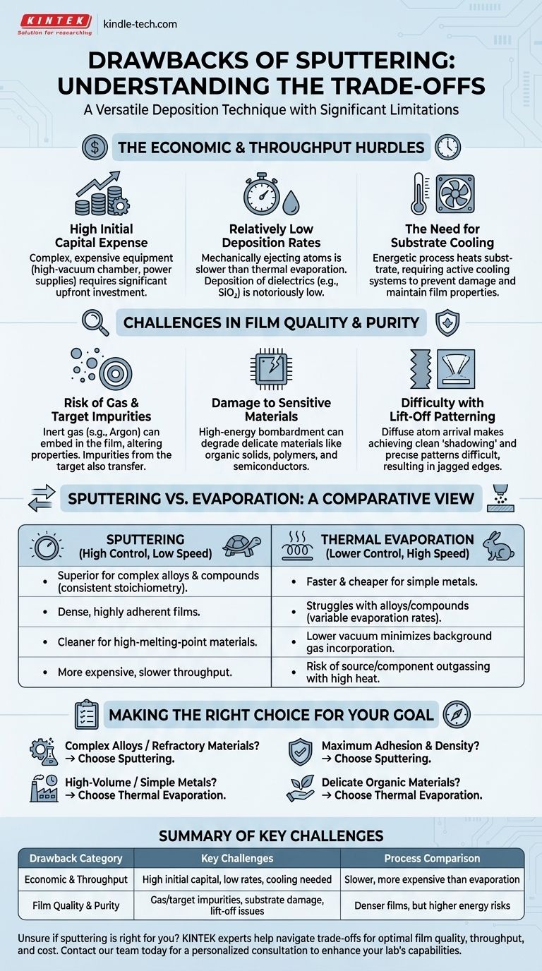
The Economic and Throughput Hurdles
For many projects, the most immediate drawbacks of sputtering are related to cost and speed. These factors can make it a non-starter for high-volume, low-margin applications.
High Initial Capital Expense
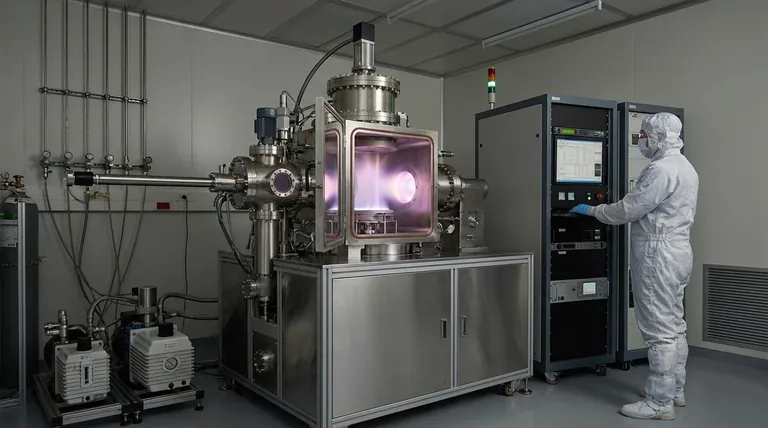
The equipment required for a sputtering system is complex and therefore expensive. A high-vacuum chamber, powerful gas-handling systems, and specialized power supplies (particularly for RF sputtering) represent a significant upfront investment.
Relatively Low Deposition Rates
Sputtering is fundamentally a process of mechanically ejecting atoms, which is often slower than boiling them off in thermal evaporation. The deposition rates for certain materials, such as dielectrics like silicon dioxide (SiO₂), are notoriously low, impacting production throughput.
The Need for Substrate Cooling
The energy imparted by the plasma and condensing atoms heats the substrate. This requires an active cooling system to prevent damage to sensitive substrates or unwanted changes in film properties, adding complexity, cost, and potentially slowing down cycle times.
Challenges in Film Quality and Purity
While known for producing dense and adherent films, sputtering presents its own set of challenges related to contamination and material integrity.
Risk of Gas and Target Impurities
The inert gas used for sputtering (typically Argon) can become embedded in the growing film. While often a small percentage, this incorporation can alter the film's electrical, optical, or mechanical properties. Furthermore, any impurities within the source material (the target) will likely be transferred into the film.
Damage to Sensitive Materials
Sputtering is an energetic, high-impact process. The bombardment of the substrate by sputtered atoms and neutral gas atoms can damage delicate materials. Organic solids, certain polymers, and sensitive semiconductor structures can be easily degraded.
Difficulty with Lift-Off Patterning
The atoms ejected from a sputter target travel diffusely, meaning they arrive at the substrate from many angles. This makes it difficult to achieve the clean "shadowing" required for photolithographic lift-off processes, often resulting in jagged edges or "fences" that prevent a clean pattern.
Understanding the Trade-offs: Sputtering vs. Evaporation
Many of sputtering's drawbacks are best understood in comparison to its main alternative in physical vapor deposition: thermal evaporation.
Control vs. Speed
Thermal evaporation is generally faster and cheaper. However, it struggles to deposit alloys and compounds with consistent composition (stoichiometry) because materials with different vapor pressures evaporate at different rates.
Sputtering excels here. It ejects atoms based on momentum transfer, not temperature, preserving the composition of a compound or alloy target in the final film. It also produces denser, more adherent films due to the higher energy of the depositing atoms.
The Purity Paradox
Evaporation typically operates under a higher vacuum (lower pressure) than sputtering. This reduces the chance of incorporating background gas into the film.
However, sputtering is a cleaner process for depositing high-melting-point (refractory) metals, as it avoids the intense heating that can cause the source crucible and surrounding components to outgas impurities in an evaporator.
Making the Right Choice for Your Goal
Selecting the correct deposition method requires matching the process capabilities to your primary objective.
- If your primary focus is depositing complex alloys or refractory materials: Sputtering is the superior choice for maintaining compositional control and depositing high-melting-point materials.
- If your primary focus is high-volume, cost-sensitive production of simple metals: Thermal evaporation is likely the faster, more economical option if ultimate film density is not critical.
- If your primary focus is maximum film adhesion and density: Sputtering's energetic deposition process creates robust, dense films that adhere strongly to the substrate.
- If your primary focus is depositing on delicate organic materials: The high-energy nature of sputtering may cause damage, making low-energy methods like thermal evaporation a safer choice.
By understanding these inherent drawbacks, you can effectively decide when to leverage sputtering for its strengths and when to select an alternative better suited to your specific technical and economic goals.
Summary Table:
| Drawback Category | Key Challenges |
|---|---|
| Economic & Throughput | High initial capital expense, relatively low deposition rates, need for substrate cooling |
| Film Quality & Purity | Risk of gas/target impurities, potential damage to sensitive substrates, difficulty with lift-off patterning |
| Process Comparison | Slower and more expensive than thermal evaporation for some applications |
Unsure if sputtering is the right thin-film deposition method for your specific application? The experts at KINTEK are here to help. We specialize in lab equipment and consumables, offering tailored solutions for your laboratory's unique challenges.
We can help you navigate the trade-offs between sputtering and other techniques like thermal evaporation to ensure you achieve the optimal balance of film quality, throughput, and cost for your research or production goals.
Contact our team today for a personalized consultation and discover how KINTEK can enhance your lab's capabilities and efficiency.
Visual Guide
Related Products
- Lab Sterile Slapping Type Homogenizer for Tissue Mashing and Dispersing
- Spark Plasma Sintering Furnace SPS Furnace
- Single Punch Manual Tablet Press Machine TDP Tablet Punching Machine
People Also Ask
- What is the primary function of an ultrasonic cleaner in coating? Achieve Unmatched Substrate Purity for PVD Adhesion
- How does a laboratory automatic masticator or homogenizer facilitate the processing of biofilm samples? Optimize Accuracy
- How does a homogenizer affect the quality of electrode slurry? Master Battery Consistency with High-Shear Mixing
- What role does an ultrasonic cleaner play in the pre-treatment of 4140 steel? Ensure Uniform Nitriding Activation
- How do ultrasonic cell disruptors or dispersion equipment function during ZIF-8 synthesis? Master Acoustic Cavitation


